NI 6528/6529 User Guide and Specifications 4 ni.com
• NI-DAQmx examples for ANSI C are in the
NI-DAQ\Examples\DAQmx ANSI C Dev directory
• Traditional NI-DAQ (Legacy) examples for ANSI C are in the
NI-DAQ\Examples\VisualC directory
For additional examples, refer to
zone.ni.com.
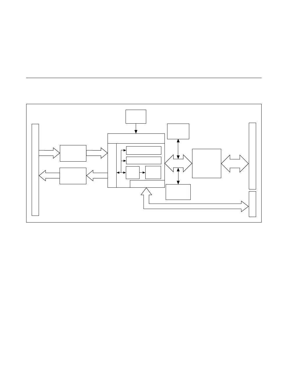
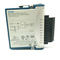
Functional Overview
Figures 1 and 2 illustrate the key functional components of the
NI 6528/6529 device.
Figure 1. NI 6528 Block Diagram
PCI Bus
Interface
Flash
Memory
Configuration
Control
Data/Control
Data/Control
24 Outputs 24 Outputs
Output Buffers
and Isolation
Input
Isolation
24 Inputs 24 Inputs
Industrial Digital
I/O Control FPGA
DIO Lines
Programmable
Power-Up States
Watchdog Timer
Change
Detection
Digital
Filtering
RTSI
PCI/PXI/CompactPCI Bus
I/O Connector
10 MHz
Clock
RTSI
RTSI