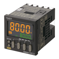
H5CC
9
Connections
Block Diagram
Terminal Arrangement
Confirm that the power supply meets specifications before use.
Note: Do not connect unuse
d terminals as relay terminals.
Transistor Output
H5CC-A/AD H5CC-AS/ASD H5CC-AU/AUD H5CC-AWSD
H5CC-A11/A11D/A11F H5CC-A11S/A11SD
H5CC-L8/L8D H5CC-L8S/L8SD H5CC-L8E/L8ED/L8EF
Output circuit
(See note.)
Internal control
circuit
Display circuit
Key switch circuit
Input circuits
Power supply
circuit
(Basic insulation)
(Basic insulation)
Note: Basic insulation is provided between
the power supply circuit and the input
circuits. However, basic insulation is
not provided in the H5CC-@F.
6789
Contact output
(+)(-)
0 V
12345
Reset
Signal
Gate
6789
Transistor output
0 V
12345
Reset
Signal
Gate
(+)(-)
6789
11
12 VDC
(-)
(+)
0 V
12345
OUT1
OUT2
(+)(-)
Reset
Signal
Gate
External
power supply
Sensor
12 13
678910
12 13 OUT1
OUT2
0 V
12345
(+)
(-)
Reset input
Reset input
Signal input
Gate input
Note: Terminals 7 and 10 have the same reset
function. The same function will be
performed whichever terminal is connected.
Terminals 7 and 10 are not connected
internally, however, so do not use them for
cross-over wiring.
6
7
8
9
10
11
1
2
3
4
5
0 V
Reset
Signal
Gate
Internal circuit
Unused
Unused
Contact
output
(-) (+)
6
7
8
9
10
11
1
2
3
4
5
0 V
Reset
Signal
Gate
Internal circuit
Unused
Unused
Transistor
output
(-) (+)
4
3
2
1 8
7
6
5
0 V
Signal
Reset
Internal circuit
Contact
output
(-) (+)
4
3
2
1 8
7
6
5
0 V
Signal
Reset
Internal circuit
Unused
Transistor
output
(-) (+)
4
3
2
1 8
7
6
5
(–) (+)
Internal circuit Internal circuit
Instantaneous
contact output
OUT1
Time-limit
contact
output
OUT2
Power for load
+
Load
Power for load
+
Load
NPN Output PNP Output
• The transistor output of the
H5CC is insulated from the
internal circuitry by a
photocoupler, so the transistor
output can be used as both
NPN and PNP output.
Power for load
+
Timer
Inductive
load
• The diode connected to the
collector of the output
transistor is used to absorb
inverted voltage that is
generated when an
inductive load is connected
to the H5CC.