Appendices
A-14
NJ-series CPU Unit Hardware User’s Manual (W500)
* The ON response time will be 120 s maximum and OFF response time will be 400 s maximum even if the response times
are set to 0 ms due to internal element delays.
Note Observe the following restrictions when connecting to a 2-wire sensor.
• Make sure the input power supply voltage is larger than the ON voltage (19 V) plus the residual voltage of the sen-
sor (approx. 3 V).
• Use a sensor with a minimum load current of 3 mA min.
• Connect bleeder resistance if you connect a sensor with a minimum load current of 5 mA or higher.
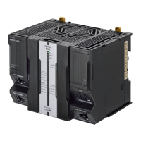
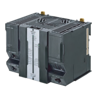
External connection
and terminal-device
variable diagram
CN1 CN2
• The input power polarity can be connected in either
direction.
• Be sure to wire both pins 23 and 24 (COM0) of
CN1, and set the same polarity for both pins.
• Be sure to wire both pins 3 and 4 (COM1) of CN1,
and set the same polarity for both pins.
• The input power polarity can be connected in either
direction.
• Be sure to wire both pins 23 and 24 (COM2) of CN2,
and set the same polarity for both pins.
• Be sure to wire both pins 3 and 4 (COM3) of CN2, and
set the same polarity for both pins.
24 VDC
24 VDC
Wd m+1
Wd m+1
Wd m
Wd m
Signal
name
Signal
name
Connec-
tor pin
Allocated
CIO word
Allocated
CIO word
1
NC
3
5
7
9
11
13
15
17
19
21
23
25
27
29
31
33
35
37
NC
39
2
4
NC
6
8
10
12
14
16
18
COM1
20
22
24
26
28
30
32
34
36
38
40
COM1
NC
COM0
COM0
Jxx_Ch1_In00
Jxx_Ch1_In01
Jxx_Ch1_In02
Jxx_Ch1_In03
Jxx_Ch1_In04
Jxx_Ch1_In05
Jxx_Ch1_In06
Jxx_Ch1_In07
Jxx_Ch2_In00
Jxx_Ch2_In01
Jxx_Ch2_In02
Jxx_Ch2_In03
Jxx_Ch2_In04
Jxx_Ch2_In05
Jxx_Ch2_In06
Jxx_Ch2_In07
Jxx_Ch2_In08
Jxx_Ch2_In09
Jxx_Ch2_In10
Jxx_Ch2_In11
Jxx_Ch2_In12
Jxx_Ch2_In13
Jxx_Ch2_In14
Jxx_Ch2_In15
Jxx_Ch1_In08
Jxx_Ch1_In09
Jxx_Ch1_In10
Jxx_Ch1_In11
Jxx_Ch1_In12
Jxx_Ch1_In13
Jxx_Ch1_In14
Jxx_Ch1_In15
Wd m+3
Wd m+3
Wd m+2
Wd m+2
24 VDC
24
VDC
Signal
name
Signal
name
Connec-
tor pin
Allocated
CIO word
Allocated
CIO word
40
38
36
34
32
30
28
26
24
22
20
18
16
14
12
10
8
6
4
NC
2
COM3
39
37
35
33
31
29
27
25
23
COM2
21
19
17
15
13
11
9
7
5
3
NC
1
COM3
COM2
NC
Jxx_Ch3_In15
Jxx_Ch3_In14
Jxx_Ch3_In13
Jxx_Ch3_In12
Jxx_Ch3_In11
Jxx_Ch3_In10
Jxx_Ch3_In09
Jxx_Ch3_In08
Jxx_Ch4_In15
Jxx_Ch4_In14
Jxx_Ch4_In13
Jxx_Ch4_In12
Jxx_Ch4_In11
Jxx_Ch4_In10
Jxx_Ch4_In09
Jxx_Ch4_In08
Jxx_Ch4_In07
Jxx_Ch4_In06
Jxx_Ch4_In05
Jxx_Ch4_In04
Jxx_Ch4_In03
Jxx_Ch4_In02
Jxx_Ch4_In01
Jxx_Ch4_In00
Jxx_Ch3_In07
Jxx_Ch3_In06
Jxx_Ch3_In05
Jxx_Ch3_In04
Jxx_Ch3_In03
Jxx_Ch3_In02
Jxx_Ch3_In01
Jxx_Ch3_In00
NC
 Loading...