Appendices
A-28
NJ-series CPU Unit Hardware User’s Manual (W500)
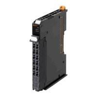
CJ1W-OD234 Transistor Output Unit (32 Points)
Circuit Configuration
External connection and ter-
minal-device variable dia-
gram
• When wiring, pay careful attention to the polarity of the external power supply. The load may operate
incorrectly if the polarity is reversed.
• Be sure to wire both terminals 23 and 24 (COM0).
• Be sure to wire both terminals 3 and 4 (COM1).
• Be sure to wire both terminals 21 and 22 (+V).
• Be sure to wire both terminals 1 and 2 (+V).
Name 32-point Transistor Output Unit with MIL Connector (Sinking Outputs)
Model CJ1W-OD234
Rated Voltage 24 VDC
Operating Load Voltage Range 20.4 to 26.4 VDC
Maximum Load Current 0.5 A/point, 2 A/common, 4 A/Unit
Maximum Inrush Current 4.0 A/point, 10 ms max.
Leakage Current 0.1 mA max.
Residual Voltage 1.5 V max.
ON Response Time 15 s max.
OFF Response Time 80 s max.
Insulation Resistance 20 M between the external terminals and the GR terminal (100 VDC)
Dielectric Strength
1,000 VAC between the external terminals and the GR terminal for 1 minute at a leakage current of 10
mA max.
Number of Circuits 32 (16 points/common, 2 circuits)
Wd m+1
Wd m
to
to
Output indicator
Internal circuits
Allocated
CIO word
Signal
name
Jxx_Ch1_Out00
+V
Jxx_Ch1_Out15
COM0
Jxx_Ch2_Out00
+V
Jxx_Ch2_Out15
COM1
COM0
COM1
SW
Wd m+1
Wd m
Wd m+1
Wd m
12 to
24 VDC
12 to
24 VDC
Signal
name
Signal
name
Connec-
tor pin
Allocated
CIO word
Allocated
CIO word
40
38
36
34
32
30
28
26
24
22
20
18
16
14
12
10
8
6
4
2
39
37
35
33
31
29
27
25
23
21
19
17
15
13
11
9
7
5
3
1
L
L
L
L
L
L
L
L
L
L
L
L
L
L
L
L
L
L
L
L
L
L
L
L
L
L
L
L
L
L
L
L
Jxx_Ch2_Out00
Jxx_Ch2_Out01
Jxx_Ch2_Out02
Jxx_Ch2_Out03
Jxx_Ch2_Out04
Jxx_Ch2_Out05
Jxx_Ch2_Out06
+V
COM1
Jxx_Ch2_Out08
Jxx_Ch2_Out09
Jxx_Ch2_Out10
Jxx_Ch2_Out11
Jxx_Ch2_Out12
Jxx_Ch2_Out07
Jxx_Ch2_Out13
Jxx_Ch2_Out14
Jxx_Ch2_Out15
+V
COM1
+V
+V
Jxx_Ch1_Out00
Jxx_Ch1_Out01
Jxx_Ch1_Out02
Jxx_Ch1_Out03
Jxx_Ch1_Out04
Jxx_Ch1_Out05
Jxx_Ch1_Out06
Jxx_Ch1_Out07
Jxx_Ch1_Out08
Jxx_Ch1_Out09
Jxx_Ch1_Out10
Jxx_Ch1_Out11
Jxx_Ch1_Out12
Jxx_Ch1_Out13
Jxx_Ch1_Out14
Jxx_Ch1_Out15
COM0 COM0
 Loading...