A-31
Appendices
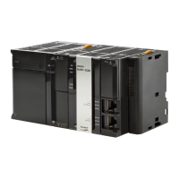
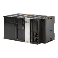
NJ-series CPU Unit Hardware User’s Manual (W500)
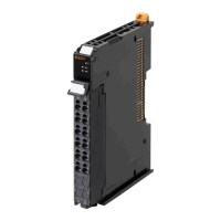
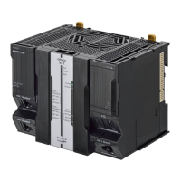
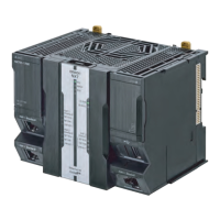
A-2 Specifications of Basic I/O Units
A
A-2-2 Basic I/O Units
External connec-
tion and terminal-
device variable
diagram
CN1 CN2
• When wiring, pay careful attention to the polarity of the
external power supply. The load may operate incor-
rectly if the polarity is reversed.
• Be sure to wire both terminals A9 and A19 (COM0) of
CN1.
• Be sure to wire both terminals B9 and B19 (COM1) of
CN1.
• Be sure to wire both terminals A10 and A20 (+V) of
CN1.
• Be sure to wire both terminals B10 and B20 (+V) of
CN1.
• When wiring, pay careful attention to the polarity of the
external power supply. The load may operate incor-
rectly if the polarity is reversed.
• Be sure to wire both terminals A9 and A19 (COM2) of
CN2.
• Be sure to wire both terminals B9 and B19 (COM3) of
CN2.
• Be sure to wire both terminals A10 and A20 (+V) of
CN2.
• Be sure to wire both terminals B10 and B20 (+V) of
CN2.
12 to
24
VDC
Wd m
Wd m+1
12 to
24
VDC
Wd m+1
Wd m
Signal
name
Signal
name
Connec-
tor pin
Allocated
CIO word
Allocated
CIO word
COM0
+V
COM0
+V
COM1
+V
Jxx_Ch2_Out08
Jxx_Ch2_Out09
Jxx_Ch2_Out10
Jxx_Ch2_Out11
Jxx_Ch2_Out12
Jxx_Ch2_Out13
Jxx_Ch2_Out14
Jxx_Ch2_Out15
COM1
+V
L
L
L
L
L
L
L
L
L
L
L
L
L
L
L
L
L
L
L
L
L
L
L
L
L
L
L
L
L
L
L
L
Jxx_Ch2_Out00
Jxx_Ch2_Out01
Jxx_Ch2_Out02
Jxx_Ch2_Out03
Jxx_Ch2_Out04
Jxx_Ch2_Out05
Jxx_Ch2_Out06
Jxx_Ch2_Out07
Jxx_Ch1_Out00
Jxx_Ch1_Out01
Jxx_Ch1_Out02
Jxx_Ch1_Out03
Jxx_Ch1_Out04
Jxx_Ch1_Out05
Jxx_Ch1_Out06
Jxx_Ch1_Out07
Jxx_Ch1_Out08
Jxx_Ch1_Out09
Jxx_Ch1_Out10
Jxx_Ch1_Out11
Jxx_Ch1_Out12
Jxx_Ch1_Out13
Jxx_Ch1_Out14
Jxx_Ch1_Out15
A20
A19
A18
A17
A16
A15
A14
A13
A12
A11
A10
A9
A8
A7
A6
A5
A4
A3
A2
A1
B20
B19
B18
B17
B16
B15
B14
B13
B12
B11
B10
B9
B8
B7
B6
B5
B4
B3
B2
B1
12 to
24
VDC
Wd m+3
Wd m+2
Wd m+2
Wd m+3
12 to
24
VDC
Signal
name
Signal
name
Connec-
tor pin
Allocated
CIO word
Allocated
CIO word
L
L
L
L
L
L
L
L
L
L
L
L
L
L
L
L
L
L
L
L
L
L
L
L
L
L
L
L
L
L
L
L
A1
A2
A3
A4
A5
A6
A7
A8
A9
A10
A11
A12
A13
A14
A15
A16
A17
A18
A19
A20
B1
B2
B3
B4
B5
B6
B7
B8
B9
B10
B11
B12
B13
B14
B15
B16
B17
B18
B19
B20
COM3
+V
COM3
+V
COM2
+V
Jxx_Ch3_Out08
Jxx_Ch3_Out09
Jxx_Ch3_Out10
Jxx_Ch3_Out11
Jxx_Ch3_Out12
Jxx_Ch3_Out13
Jxx_Ch3_Out14
Jxx_Ch3_Out15
COM2
+V
Jxx_Ch3_Out00
Jxx_Ch3_Out01
Jxx_Ch3_Out02
Jxx_Ch3_Out03
Jxx_Ch3_Out04
Jxx_Ch3_Out05
Jxx_Ch3_Out06
Jxx_Ch3_Out07
Jxx_Ch4_Out00
Jxx_Ch4_Out01
Jxx_Ch4_Out02
Jxx_Ch4_Out03
Jxx_Ch4_Out04
Jxx_Ch4_Out05
Jxx_Ch4_Out06
Jxx_Ch4_Out07
Jxx_Ch4_Out08
Jxx_Ch4_Out09
Jxx_Ch4_Out10
Jxx_Ch4_Out11
Jxx_Ch4_Out12
Jxx_Ch4_Out13
Jxx_Ch4_Out14
Jxx_Ch4_Out15
 Loading...