Appendices
A-36
NJ-series CPU Unit Hardware User’s Manual (W500)
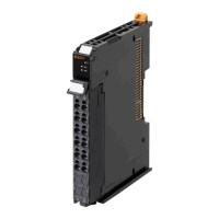
CJ1W-OD204 Transistor Output Unit (8 Points)
* Terminal numbers A0 to A8 and B0 to B8 are used in the external connection and terminal-device variable diagrams. They are not printed
on the Units.
Name 8-point Transistor Output Unit with Terminal Block (Sourcing Outputs)
Model CJ1W-OD204
Rated Voltage 24 VDC
Operating Load Voltage Range 20.4 to 26.4 VDC
Maximum Load Current 0.5 A/point, 4.0 A/Unit
Leakage Current 0.1 mA max.
Residual Voltage 1.5 V max.
ON Response Time 0.5 ms max.
OFF Response Time 1.0 ms max.
Load Short-circuit Protection
Detection current: 0.7 to 2.5 A
Automatic restart after error clearance. (Refer to page A-98.)
Insulation Resistance 20 M between the external terminals and the GR terminal (100 VDC)
Dielectric Strength
1,000 VAC between the external terminals and the GR terminal for 1 minute at a leakage cur-
rent of 10 mA max.
Number of Circuits 8 (8 points/common, 1 circuit)
Internal Current Consumption 100 mA max.
Fuse None
External Power Supply 20.4 to 26.4 VDC, 40 mA min.
Weight 120 g max.
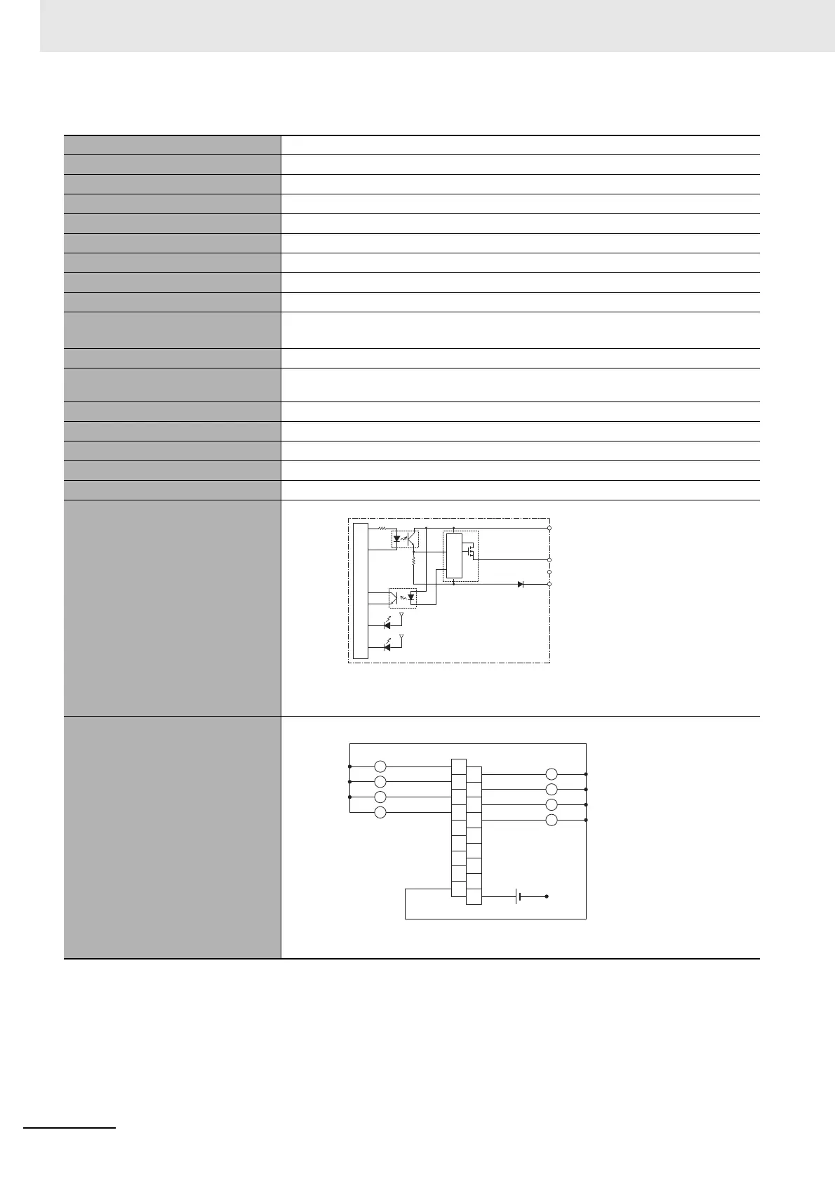
Circuit Configuration
• When an overcurrent is detected, the ERR indicator will light. At the same time, the corre-
sponding bit in the Basic I/O Unit Information Area system-defined variable will change to
TRUE.
External connection and terminal-
device variable diagram
• When wiring, pay careful attention to the polarity of the external power supply. The load may
operate incorrectly if the polarity is reversed.
Output indicator
ERR indicator
Internal circuits
to
Signal name
COM (+V)
Jxx_Ch1_Out00
Jxx_Ch1_Out07
0 V
Short-circuit
protection
24 VDC
Signal
name
Signal
name
Connec-
tor pin
*
B1
Jxx_Ch1_Out01
B2
Jxx_Ch1_Out03
B3
Jxx_Ch1_Out05
B4
Jxx_Ch1_Out07
B5
B6
B7
B8
A1
Jxx_Ch1_Out00
A2
Jxx_Ch1_Out02
A3
Jxx_Ch1_Out04
A4
Jxx_Ch1_Out06
A5
NC
A6
A7
A8
0 V
B0
A0
COM (+V)
L
L
L
L
L
L
L
L
NC
NC
NC
NC
NC
NC
NC
 Loading...