A-5VL
IC BLOCK DIAGRAM/ TERMINAL DESCRIPTION
Q203/Q204: PCM1796DB AUDIO DIGITAL to ANALOG CONVERTER-2
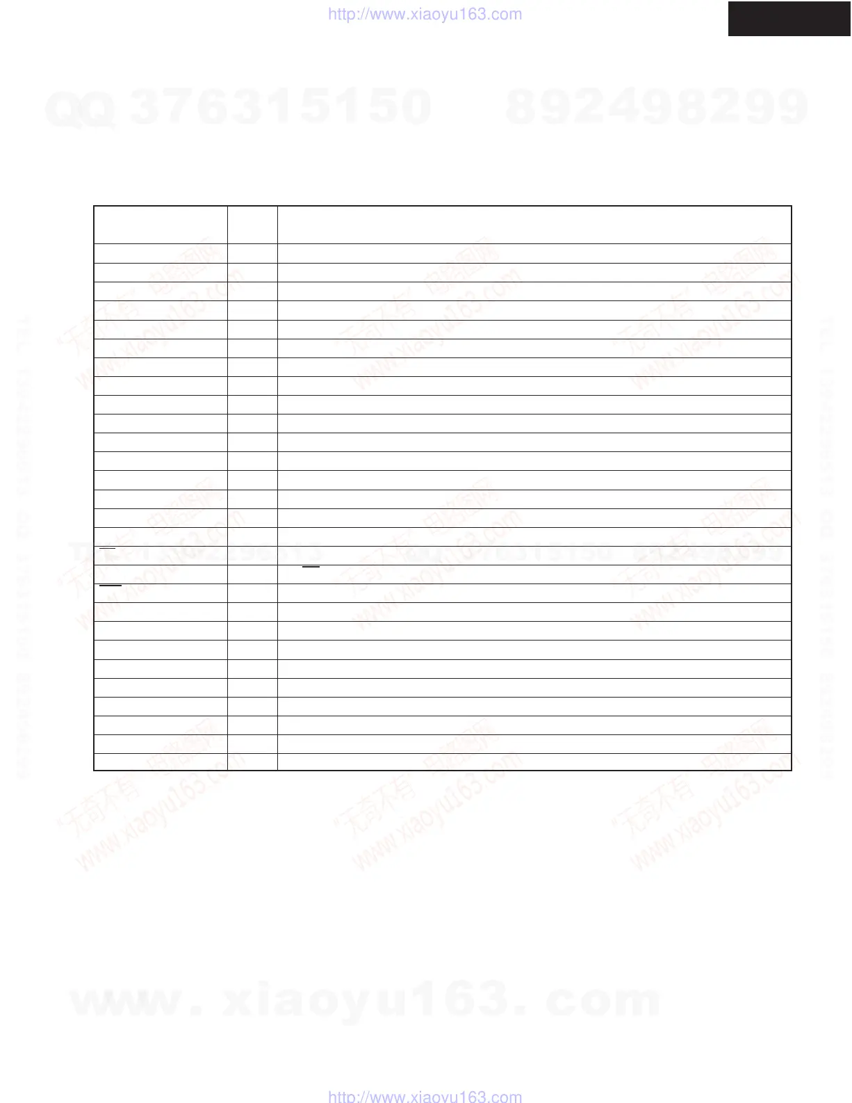
TERMINAL
I/O DESCRIPTIONS
NAME PIN
I/O DESCRIPTIONS
AGND1 19 – Analog ground (internal bias)
AGND2 24 – Analog ground (internal bias)
AGND3L 27 – Analog ground (L-channel DACFF)
AGND3R 16 – Analog ground (R-channel DACFF)
BCK 6 I Bit clock input
(1)
DATA 5 I Serial audio data input
(1)
DGND 8 – Digital ground
I
OUT
L+ 25 O L-channel analog current output+
I
OUT
L– 26 O L-channel analog current output–
I
OUT
R+ 17 O R-channel analog current output+
I
OUT
R– 18 O R-channel analog current output–
I
REF
20 – Output current reference bias pin
LRCK 4 I Left and right clock (f
S
) input
(1)
MC 12 I Mode control clock input
(1)
MDI 11 I Mode control data input
(1)
MDO 13 I/O Mode control readback data output
(3)
MS 10 I/O Mode control chip-select input
(2)
MSEL 3 I I
2
C/SPI select
(1)
RST 14 I Reset
(1)
SCK 7 I System clock input
(1)
V
CC
1 23 – Analog power supply, 5 V
V
CC
2L 28 – Analog power supply (L-channel DACFF), 5 V
V
CC
2R 15 – Analog power supply (R-channel DACFF), 5 V
V
COM
L 22 – L-channel internal bias decoupling pin
V
COM
R 21 – R-channel internal bias decoupling pin
V
DD
9 – Digital power supply, 3.3 V
ZEROL 1 I/O Zero flag for L-channel
(2)
ZEROR 2 I/O Zero flag for R-channel
(2)
(1)
Schmitt-trigger input, 5-V tolerant
(2)
Schmitt-trigger input and output. 5-V tolerant input and CMOS output
(3)
Schmitt-trigger input and output. 5-V tolerant input. In I
2
C mode, this pin becomes an open-drain 3-state output; otherwise, this pin is a CMOS
output.
TERMINAL DESCRIPTION
w
w
w
.
x
i
a
o
y
u
1
6
3
.
c
o
m
Q
Q
3
7
6
3
1
5
1
5
0
9
9
2
8
9
4
2
9
8
T
E
L
1
3
9
4
2
2
9
6
5
1
3
9
9
2
8
9
4
2
9
8
0
5
1
5
1
3
6
7
3
Q
Q
TEL 13942296513 QQ 376315150 892498299
TEL 13942296513 QQ 376315150 892498299
http://www.xiaoyu163.com
http://www.xiaoyu163.com
 Loading...