EasyManua.ls Logo

Onkyo HT-R430 Service Manual

Onkyo HT-R430
152 pages
To Next Page IconTo Next Page
Page #1 background imageLoading...
Page #1 background image
HT-R430
SERVICE MANUAL
SERVICE MANUAL
Black and Silver models
Ref. No. 3866
052005
AV RECEIVER
120V AC, 60HzS MDD
230-240V AC, 50HzS MPA
MODEL HT-R430
120V AC, 60HzB MDD
230-240V AC, 50HzB MPA
TONE
+
STEREO
LISTENING MODE
DISPLAY
DIGITAL INPUT
DIMMER MEMORY
TUNING MODE
RETURN
TUNING / PRESET
ENTER
SETUP
STANDBY
STANDBY/ON
CLEAR
PHONES
MULTl CH DVD VIDEO 1/VCR VIDEO 2 VIDEO 3 TAPE TUNER CD
MASTER VOLUME
A SPEAKERS B
RC-606S
MUTING
MENUTOP MENU
SP A
/
B
SETUPRETURN
RANDOM
SUBTITLE
PLAY MODE
AUDIO REPEAT
RC
-
606S
--
/
---
TAPE/AMP
ON STANDBY
DIMMER SLEEP
INPUT SELECTOR
REMOTE MODE
V
1
V
2
V
3
C
DTAPE TUNER
DVD
MULTI CH
LISTENING MODE
DISPLAY
TEST
TONE
CH SEL
SURROUND
STEREO
CINE FLTR
LEVEL
+
LEVEL
-
L NIGHT
OR-EQ
VOL
CDR
MD
DVD
RECEIVER
C
D
+
10
0
CLR
123
456
789
ENTER
CH
DISC
SAFETY-RELATED COMPONENT
WARNING!!
COMPONENTS IDENTIFIED BY MARK ON THE
SCHEMATIC DIAGRAM AND IN THE PARTS LIST ARE
CRITICAL FOR RISK OF FIRE AND ELECTRIC SHOCK.
REPLACE THESE COMPONENTS WITH ONKYO
PARTS WHOSE PART NUMBERS APPEAR AS SHOWN
IN THIS MANUAL.
MAKE LEAKAGE-CURRENT OR RESISTANCE
MEASUREMENTS TO DETERMINE THAT EXPOSED
PARTS ARE ACCEPTABLY INSULATED FROM THE
SUPPLY CIRCUIT BEFORE RETURNING THE
APPLIANCE TO THE CUSTOMER.
w
w
w
.
x
i
a
o
y
u
1
6
3
.
c
o
m
Q
Q
3
7
6
3
1
5
1
5
0
9
9
2
8
9
4
2
9
8
T
E
L
1
3
9
4
2
2
9
6
5
1
3
9
9
2
8
9
4
2
9
8
0
5
1
5
1
3
6
7
3
Q
Q
TEL 13942296513 QQ 376315150 892498299
http://www.xiaoyu163.com
Question and Answer IconNeed help?

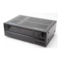
Do you have a question about the Onkyo HT-R430 and is the answer not in the manual?

Onkyo HT-R430 Specifications

General IconGeneral
Channels5.1
HDMI Inputs4
HDMI Outputs1
Audio Formats SupportedDolby Digital, DTS
Speaker impedance6 - 16 Ohms
Input sensitivity (line)200 mV
Signal to noise ratio (line)100 dB
Signal-to-Noise Ratio100 dB
Output (line)200 mV
Video ConnectionsHDMI, Composite
Video Inputs/Outputs4/1
Audio Inputs/Outputs4/1
Total Harmonic Distortion0.08%
Frequency Response10 Hz - 100 kHz
Input Sensitivity and Impedance200 mV / 47 kOhms
Tuning rangeFM/AM

Summary

Safety Warnings

Specifications

Amplifier Section

Detailed electrical and performance specifications for the amplifier.

Video Section

Specifications related to video signal input/output characteristics.

Tuner Section

Specifications for FM and AM tuner performance.

General Specifications

Overall unit specifications including power, dimensions, and weight.

Video Inputs

List of supported video input formats and connectors.

Video Outputs

List of supported video output formats and connectors.

Audio Inputs

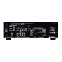
List of supported audio input types and connectors.

Audio Outputs

List of supported audio output types and connectors.

Service Procedures

Replacing Fuses

Procedure for safely replacing fuses, emphasizing correct type and rating.

Unit Initialization and Memory Backup

Procedures for resetting the unit and managing memory backup system.

Operation Check-1: Speaker Protect-1 (DC Voltage Detection)

Operation Check-2: Speaker Protect-2 (Current Detection)

Operation Check-3: Power Supply and Thermal Sensors

Output Sensor Check

Procedure to verify the output sensor operation by adjusting volume.

Thermal Sensor Check

Procedure to check the thermal sensor by verifying temperature readings.

Operation Check-4: DSP Debug Mode

Entering DSP Debug Mode

Procedure to enter DSP debug mode for operation checks.

Exploded Views-1

Exploded Views-2

Block Diagram

Schematic Diagrams-1: Audio Input Section

Audio Input Circuitry

Detailed schematic of the audio signal input circuitry.

Schematic Diagrams-2: DSP Section

DSP Circuitry

Detailed schematic of the Digital Signal Processor circuit.

Schematic Diagrams-3: Driver Amplifier Section

Driver Amplifier Stages

Detailed schematic of the amplifier driver stages for speaker outputs.

Schematic Diagrams-4: Power Amplifier Section

Power Amplifier Stages

Detailed schematic of the main power amplifier stages.

Schematic Diagrams-5: Speaker Terminal Section

Speaker Terminal Connections

Schematic showing connections to speaker terminals and protection circuits.

Schematic Diagrams-6: Power Supply Section

Power Supply Circuitry

Schematic of the unit's power supply circuits and transformers.

Schematic Diagrams-7: Display Section

Display Circuitry

Schematic of the front panel display and related control circuits.

Schematic Diagrams-8: Video Section

Video Circuitry

Schematic of the video processing and switching circuitry.

PC Board Connection Diagram

Printed Circuit Board Views-1

U01 Display PC Board (NADIS-8513) Side A

Top-side component layout of the display control PCB.

Printed Circuit Board Views-2

U01 Display PC Board (NADIS-8513) Side B

Bottom-side component layout of the display control PCB.

Printed Circuit Board Views-3

U02 DSP PC Board (NADG-8514) Side A

Top-side component layout of the DSP processing PCB.

Printed Circuit Board Views-4

U02 DSP PC Board (NADG-8514) Side B

Bottom-side component layout of the DSP processing PCB.

Printed Circuit Board Views-5

U03 Switch PC Board (NASW-8515) Side A Side B

Component layout for the switch PC board (both sides).

U04 Headphone Jack PC Board (NAETC-8516) Side A Side B

Component layout for the headphone jack PC board (both sides).

Printed Circuit Board Views-6

U05 Amplifier PC Board (NAAF-8523) Component side

Component layout of the amplifier PC board (component side).

Printed Circuit Board Views-7

U05 Amplifier PC Board (NAAF-8523) Soldering side

Component layout of the amplifier PC board (soldering side).

Printed Circuit Board Views-8

U06 Sec. Terminal-2 PC Board (NAPS-8524) Component side

Component layout of the terminal PC board (component side).

U08 Thermal Sensor PC Board (NAETC-8526) Component side

Component layout of the thermal sensor PC board (component side).

Printed Circuit Board Views-9

U11 Power Supply-1 PC Board (NAPS-8544) Component side

Component layout of the power supply PC board (component side).

Printed Circuit Board Views-10

U13 Power Supply-2 PC Board (NAPS-8546) Component side

Component layout of the second power supply PC board (component side).

U14 Sec. Terminal-1 PC Board (NAPS-8547) Component side

Component layout of the terminal PC board (component side).

Printed Circuit Board Views-11

U15 Speaker Terminal PC Board (NAETC-8548) Component side

Component layout of the speaker terminal PC board (component side).

Printed Circuit Board Views-12

U16 Video PC Board (NAVD-8549) Component side

Component layout of the video PC board (component side).

Printed Circuit Board Views-13

U17 Driver Amplifier PC Board (NAAF-8550) Component side

Component layout of the driver amplifier PC board (component side).

IC Block Diagrams and Terminal Descriptions-1

Q201: CS494003CQZ (Multi-Standard Audio Decoder)-1/11

Block diagram and terminal descriptions for the CS494003 audio decoder IC.

Block Diagram

Internal functional blocks of the CS494003 audio decoder.

Pin Layout

Pinout diagram for the CS494003 audio decoder IC.

IC Block Diagrams and Terminal Descriptions-2

Q201: CS494003CQZ (Multi-Standard Audio Decoder)-2/11

Terminal descriptions for the CS494003 audio decoder IC (part 2).

Terminal Description

Detailed descriptions of various terminals on the CS494003 IC.

IC Block Diagrams and Terminal Descriptions-3

Q201: CS494003CQZ (Multi-Standard Audio Decoder)-3/11

Terminal descriptions for the CS494003 audio decoder IC (part 3).

IC Block Diagrams and Terminal Descriptions-4

Q201: CS494003CQZ (Multi-Standard Audio Decoder)-4/11

Terminal descriptions for the CS494003 audio decoder IC (part 4).

IC Block Diagrams and Terminal Descriptions-5

Q201: CS494003CQZ (Multi-Standard Audio Decoder)-5/11

Terminal descriptions for the CS494003 audio decoder IC (part 5).

IC Block Diagrams and Terminal Descriptions-6

Q201: CS494003CQZ (Multi-Standard Audio Decoder)-6/11

Terminal descriptions for the CS494003 audio decoder IC (part 6).

IC Block Diagrams and Terminal Descriptions-7

Q201: CS494003CQZ (Multi-Standard Audio Decoder)-7/11

Terminal descriptions for the CS494003 audio decoder IC (part 7).

IC Block Diagrams and Terminal Descriptions-8

Q201: CS494003CQZ (Multi-Standard Audio Decoder)-8/11

Terminal descriptions for the CS494003 audio decoder IC (part 8).

IC Block Diagrams and Terminal Descriptions-9

Q201: CS494003CQZ (Multi-Standard Audio Decoder)-9/11

Terminal descriptions for the CS494003 audio decoder IC (part 9).

IC Block Diagrams and Terminal Descriptions-10

Q201: CS494003CQZ (Multi-Standard Audio Decoder)-10/11

Terminal descriptions for the CS494003 audio decoder IC (part 10).

IC Block Diagrams and Terminal Descriptions-11

Q201: CS494003CQZ (Multi-Standard Audio Decoder)-11/11

Terminal descriptions for the CS494003 audio decoder IC (part 11).

IC Block Diagram and Terminal Descriptions-12

Q281: MX26LV040 (4M-Bit CMOS Single Voltage 3V Only High Speed Flash Memory)

Block diagram, pin layout, and terminal descriptions for the MX26LV040 flash memory.

Block Diagram

Internal functional blocks of the MX26LV040 flash memory.

Pin Layout

Pinout diagram for the MX26LV040 flash memory.

IC Block Diagrams and Terminal Descriptions-13

Q421 : CS42518 (8-Ch Codec with S/PDIF Receiver)-1/4

Block diagram for the CS42518 audio codec IC.

Block Diagram

Internal functional blocks of the CS42518 audio codec.

IC Block Diagrams and Terminal Descriptions-14

Q421 : CS42518 (8-Ch Codec with S/PDIF Receiver)-2/4

Pin layout and terminal descriptions for the CS42518 audio codec IC.

Pin Layout

Pinout diagram for the CS42518 audio codec.

Terminal Description

Detailed descriptions of the CS42518 IC terminals.

IC Block Diagrams and Terminal Descriptions-15

Q421 : CS42518 (8-Ch Codec with S/PDIF Receiver)-3/4

Terminal descriptions for the CS42518 audio codec IC (part 3).

IC Block Diagrams and Terminal Descriptions-16

Q421 : CS42518 (8-Ch Codec with S/PDIF Receiver)-4/4

Terminal descriptions for the CS42518 audio codec IC (part 4).

IC Block Diagram and Terminal Descriptions-17

Q802: M66005 (FL tube driver)

Block diagram and terminal descriptions for the M66005 FL tube driver IC.

Block Diagram

Internal functional blocks of the M66005 FL tube driver.

Terminal Description

Detailed descriptions of the M66005 IC terminals.

IC Block Diagram and Terminal Descriptions-18

Q1003, 1012, 1013 : LA7956 (Video switch)

Block diagram and truth table for the LA7956 video switch IC.

Block Diagram

Internal functional blocks of the LA7956 video switch.

Truth Table

Table showing output states based on input conditions for the LA7956.

IC Block Diagrams and Terminal Descriptions-19

Q5501: NJW1157(8-CHANNEL ELECTRONIC VOLUME WITH INPUT SELECTOR)-1/2

Block diagram for the NJW1157 volume control IC (part 1).

Block Diagram

Internal functional blocks of the NJW1157 volume control IC.

IC Block Diagrams and Terminal Descriptions-20

Q5501: NJW1157(8-CHANNEL ELECTRONIC VOLUME WITH INPUT SELECTOR)-2/2

Terminal descriptions for the NJW1157 volume control IC (part 2).

Terminal Description

Detailed descriptions of the NJW1157 IC terminals.

IC Block Diagrams and Terminal Descriptions-21

Q5502: NJU7311AM (Analog Function Switch)

Block diagram and terminal descriptions for the NJU7311AM analog switch IC.

Block Diagram

Internal functional blocks of the NJU7311AM analog switch.

Terminal Description

Detailed descriptions of the NJU7311AM IC terminals.

IC Block Diagrams and Terminal Descriptions-22

Q5640: AN34060A (3 Output Voltage Regulator)

Block diagram and terminal descriptions for the AN34060A voltage regulator IC.

Block Diagram

Internal functional blocks of the AN34060A voltage regulator.

Terminal Description

Detailed descriptions of the AN34060A IC terminals.

FL Tube View

Q801: 16BT127GNK

Diagram illustrating the front panel display segments and corresponding button labels.

Microprocessor Terminal Descriptions-1

Q701: M30622MGP-236FPU0

Terminal descriptions for the M30622MGP microprocessor (part 1).

Microprocessor Terminal Descriptions-2

Q701: M30622MGP-236FPU0

Terminal descriptions for the M30622MGP microprocessor (part 2).

Adjustment Procedure-1

Idling Current Adjustment

Procedure for adjusting the idling current for amplifier output transistors.

Adjustment Procedure-2

Idling Current Adjustment

Visual guide showing test points and trimming resistors for idling current adjustment.

Exploded View Parts List

PC Board Parts List

Related product manuals