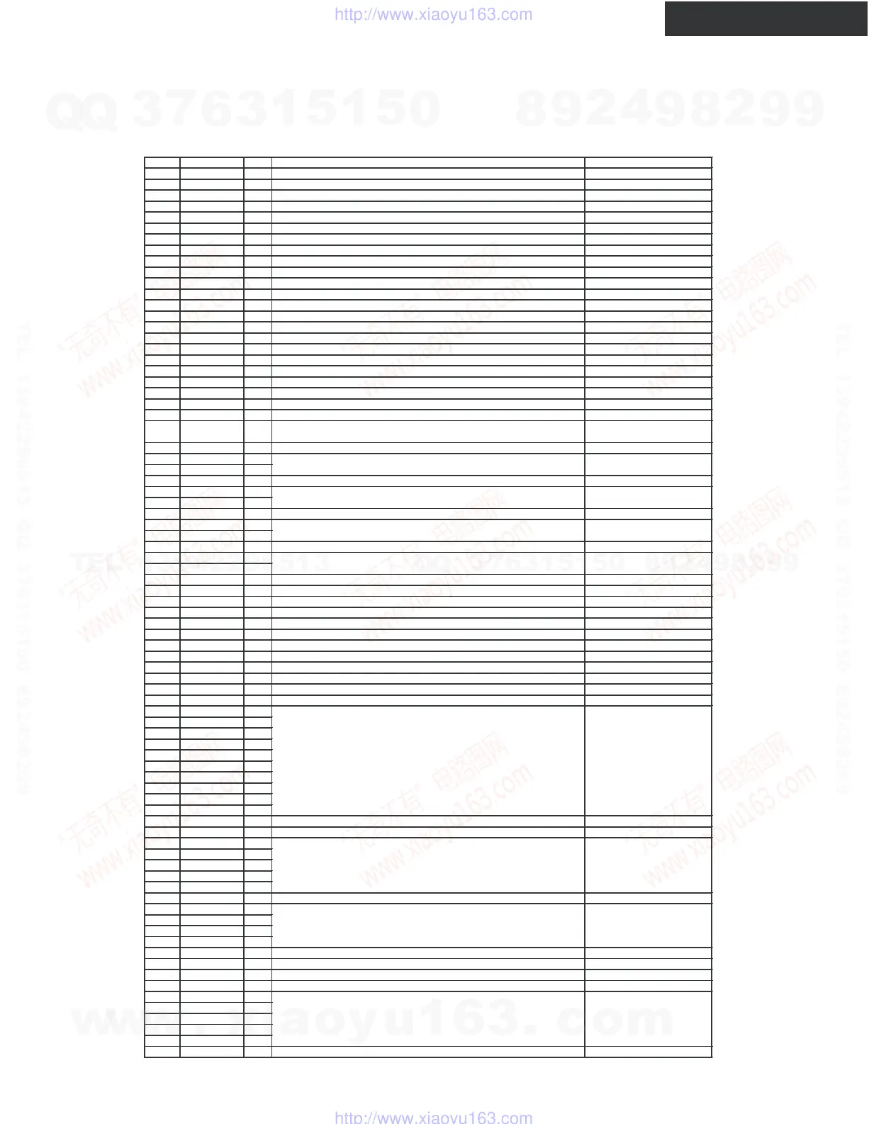
Pin # Pin Name I/O Descri
tion Use
1 HSYNC I Horizontal S
nc in
ut control si
nal Video and Audio
2VSYNC IVertical S
nc in
ut control si
nal Video and Audio
3CGND Di
ital core GND. Ground
4 CVCC18 Di
ital core VCC. Connect to 1.8V su
l
. Power
5 SPDIF I S/PDIF Audio in
ut Video and Audio
6 MCLK I Audio In
ut Master Clock Video and Audio
7 SD3 I I2S Serial Data Video and Audio
8 SD2 I I2S Serial Data Video and Audio
9 SD1 I I2S Serial Data Video and Audio
10 SD0 I I2S Serial Data Video and Audio
11 WS I I2S Word Select Video and Audio
12 SCK I I2S Serial Clock Video and Audio
13 IOVCC IO Pin VCC. Connect to 3.3V su
l
. Power
14 IOGND IO Pin GND. Ground
15 CGND Di
ital core GND. Ground
16 CVCC18 Di
ital core VCC. Connect to 1.8V su
l
. Power
17 INT O Interru
t Out
ut. Confirration/Pro
rammin
18 HPD I Hot Plu
Detect In
ut. Confirration/Pro
rammin
19 DSDA I/O DDC data Control
20 DSCL I/O DDC Clock Control
21 RSVDL I Reserved for use b
Silicon ima
e, and must be tied LOW. Confirration/Pro
rammin
22 PGND1 TMDS Core PLL Ground. Ground
23 PVCC1 TMDS Core PLL Power. Connect to 3.3V su
l
. Power
25 AGND Analo
GND. Ground
26 TXC- O
27 TXC+ O
28 AVCC Analo
VCC. Connect to 3.3Vsu
l
. Power
29 TX0- O
30 TX0+ O
31 AGND Analo
GND. Ground
32 TX1- O
33 TX1+ O
34 AVCC Analo
VCC. Connect to 3.3Vsu
l
. Power
35 TX2- O
36 TX2+ O
37 AGND Analo
GND. Ground
38 PVCC2 Filter PLL Power. Connect to 3.3V su
l
.POwer
39 PGND2 Filter PLL Ground. Ground
40 NC Not connected.
41 CI2CA I I2C device address select Control
42 RESET I Reset Pin. Active LOW Control
43 CSCL I I2C Clock Control
44 CSDA I/O I2C Data Control
45 CVCC18 Di
ital core VCC. Connect to 1.8V su
l
. Power
46 CGND Di
ital core GND. Ground
47 IOGND IO Pin GND. Ground
48 IOVCC IO Pin VCC. Connect to 3.3V su
l
. Power
49 D23 I
50 D22 I
51 D21 I
52 D20 I
53 D19 I
54 D18 I
55 D17 I
56 D16 I
57 D15 I
58 D14 I
59 CVCC18 Di
ital core VCC. Connect to 1.8V su
l
. Power
60 CGND Di
ital core GND. Ground
61 D13 I
62 D12 I
63 D11 I
64 D10 I
65 D9 I
66 IDCK I In
ut Data Clock Video and Audio
67 D8 I
68 D7 I
69 D6 I
70 D5 I
71 IOVCC IO Pin VCC. Connect to 3.3V su
l
. Power
72 IOGND IO Pin GND. Ground
73 CGND Di
ital core GND. Ground
74 CVCC18 Di
ital core VCC. Connect to 1.8V su
l
. Power
75 D4 I
76 D3 I
77 D2 I
78 D1 I
79 D0 I
80 DE I Data enable Video and Audio
Video and Audio
Video and Audio
Video and Audio
Video and Audio
12-bit Input Pixel Data Bus. These pins are used in 24-bit mode, single-
edge mode.
12-bit Input Pixel Data Bus. These pins are used in 24-bit mode, single-
edge mode.
12-bit Input Pixel Data Bus. These pins are used in 24-bit mode, single-
edge mode.
12-bit Input Pixel Data Bus. These pins are used in 24-bit mode, single-
edge mode.
24 EXT_SWING I
Voltage Swing Adjustment. The resistor between AVCC and this pin
determines the am
litude of the volta
e swin
.
Differential signal data
TMDS output clock.
TMDS output data.
TMDS output data.
TMDS output data.
Differential signal data
Differential signal data
Differential signal data
Differential si
gnal data
TX-SR604/604E/8460
IC BLOCK DIAGRAMS AND TERMINAL DESCRIPTIONS -31
Q8401 : SiI9030CTU (HDMI Transmitter)
TERMINAL DESCRIPTION
w
w
w
.
x
i
a
o
y
u
1
6
3
.
c
o
m
Q
Q
3
7
6
3
1
5
1
5
0
9
9
2
8
9
4
2
9
8
T
E
L
1
3
9
4
2
2
9
6
5
1
3
9
9
2
8
9
4
2
9
8
0
5
1
5
1
3
6
7
3
Q
Q
TEL 13942296513 QQ 376315150 892498299
TEL 13942296513 QQ 376315150 892498299
http://www.xiaoyu163.com
http://www.xiaoyu163.com
 Loading...