Pin No. Symbol I/O Description
1 VDD Power supply terminal. Connect to 5V.
2 VSS Ground terminal.
3 X1 Ceramic oscillator connection terminals for main system.
4 X2 Connect the 5MHz ceramic oscillator between #3 and #4.
5 IC/VPP Power supply terminal for flash memory IC.
6 ~RESET I System reset signal input terminal.
7 SUBCL/SCK I Clock input terminal to transmit from main microprocessor or to write the program.
8 SUBDO/SDI I Data input terminal to transmit from main microprocessor or to write the program.
9 SUBDI/SDD O Data output terminal to transmit to main microprocessor or to write the program.
10 SUBLDY O Data ready output terminal to transmit to the main microprocessor.
11 VBJ I Pulse input terminal from the rotary encoder of volume.
12 VAJ I Pulse input terminal from the rotary encoder of volume.
13 SSCBJ I Pulse input terminal from the rotary encoder of SSC.
14 SSCAJ I Pulse input terminal from the rotary encoder of SSC.
15 ~IRIN I Signal input terminal to remote controller.
16 ~IRF I Signal input terminal to remote controller.
17 STBYLED O Standby LED control output terminal.
18 AVSS Ground terminal for A/D converter.
19 K3 I Operation key connection terminal.
20 K2 I Operation key connection terminal.
21 K1 I Operation key connection terminal.
22 K0 I Operation key connection terminal.
23 VSS0 Ground terminal
24 AVDD Power supply terminal for A/D converter.
25 VDDD Power supply terminal. Apply +5V.
26 ~SYSIN I System code input terminal.
27 ~SYSOUT O System code output terminal.
28 P35 O Segment output terminal of P35.
29 P34 O Segment output terminal of P34.
30 P33 O Segment output terminal of P33.
31 P32 O Segment output terminal of P32.
32 P31 O Segment output terminal of P31.
33 P30 O Segment output terminal of P30.
34 P29 O Segment output terminal of P29.
35 P28 O Segment output terminal of P28.
36 P27 O Segment output terminal of P27.
37 P26 O Segment output terminal of P26.
38 P25 O Segment output terminal of P25.
39 P24 O Segment output terminal of P24.
40 P23 O Segment output terminal of P23.
Pin No. Symbol I/O Description
41 P22 O Segment output terminal of P22.
42 P21 O Segment output terminal of P21.
43 P20 O Segment output terminal of P20.
44 P19 O Segment output terminal of P19.
45 P18 O Segment output terminal of P18.
46 P17 O Segment output terminal of P17.
47 P16 O Segment output terminal of P16.
48 P15 O Segment output terminal of P15.
49 P14 O Segment output terminal of P14.
50 P13 O Segment output terminal of P13.
51 P12 O Segment output terminal of P12.
52 P11 O Segment output terminal of P11.
53 P10 O Segment output terminal of P10.
54 P9 O Segment output terminal of P9.
55 P8 O Segment output terminal of P8.
56 P7 O Segment output terminal of P7.
57 P6 O Segment output terminal of P6.
58 P5 O Segment output terminal of P5.
59 VDD2 Power supply termini. Apply +5V.
60 VLOAD Negative power supply terminal of FL controller.
61 P4 O Segment output terminal of P4.
62 P3 O Segment output terminal of P3.
63 P2 O Segment output terminal of P2.
64 P1 O Segment output terminal of P1.
65 16G O Grid output terminal of 16G.
66 15G O Grid output terminal of 15G.
67 14G O Grid output terminal of 14G.
68 13G O Grid output terminal of 13G.
69 12G O Grid output terminal of 12G.
70 11G O Grid output terminal of 11G.
71 10G O Grid output terminal of 10G.
72 9G O Grid output terminal of 9G.
73 8G O Grid output terminal of 8G.
74 7G O Grid output terminal of 7G.
75 6G O Grid output terminal of 6G.
76 5G O Grid output terminal of 5G.
77 4G O Grid output terminal of 4G.
78 3G O Grid output terminal of 3G.
79 2G O Grid output terminal of 2G.
80 1G O Grid output terminal of 1G.
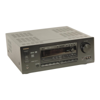
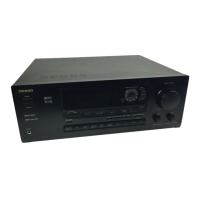
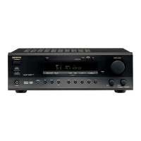
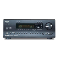
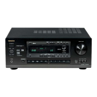
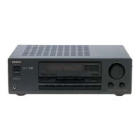
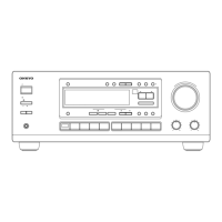
TX-DS595/696
SUB MICROPROCESSOR TERMINAL DESCRIPTIONS
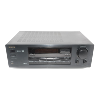
TX-DS595/696
 Loading...