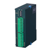
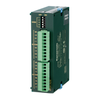
FP0 A/D Converter Unit
Specifications
7 − 4
7.1 Specifications
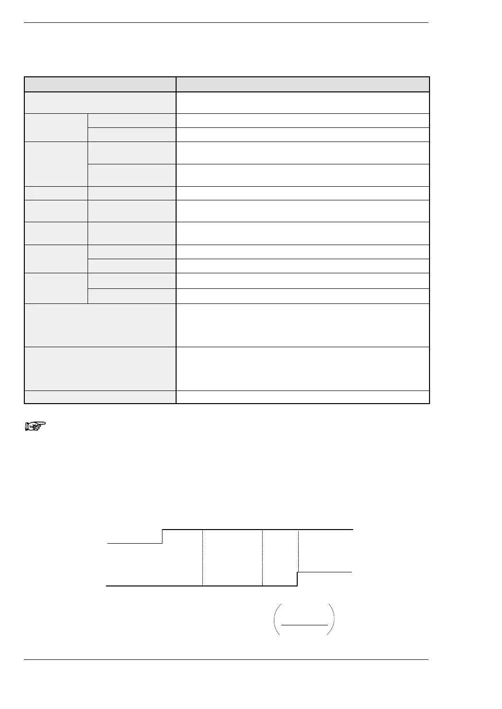
Analog input specifications
Item Description
Number of input points
8 channels/unit (the number of input points can be switched to 2, 4, 6 or
8 channels)
Voltage range 0to5V,−10 to +10 V, −100 to +100 mV
nput range
Current range 0 to 20mA
0to5V
0 to 20mA
K0 to K4000 (H0000 to H0FA0)
∗
1
g
ta
output
−10 to +10V
−100 to 100mV
K −2000 to K +2000 (HF830 to H07D0)
∗
1
Resolution Voltage/Current range 1/4000 (12bits)
Conversion
speed
Voltage/Current range
1ms/channel
∗
2
Overall
precision
Voltage/Current range
1%F.S. or less (at 0 to 55°C/32 to 131°F), 0.6% F.S. or less
(at 25°C/77°F)
In
ut
Voltage range
1MΩ or more
impedance
Current range
250Ω
Absolute
Voltage range
15V
max
mum
input
Current range +30mA
Insulation method
∗
5
⋅Between analog input terminal to FP0 internal circuit:
photocoupler insulation (non-insulated between analog inputs)
⋅Between analog input terminal to A/D converter unit external power sup-
ply: insulation-type DC/DC converter
Number of FP0 input contact points
⋅32 input contact points
First half (16 points): analog input ch0, 2, 4 and 6 data (WX2)
∗
6
Second half (16 points): analog input ch1, 3, 5 and 7 data (WX3)
∗
6}
⋅32 output contact points (Not used)
Averaging function Can be switched on and off
Notes
• (
∗
1) If the analog input value exceeds the upper/lower limit, the digital
value is held at the upper/lower limit.
• (
∗
2) The time noted below is required before the analog data is
reflected in the control unit input.
Conversion
time
Refresh
standby time
Refresh
time
K2000
Analog input
WX2
0V
K0
10V
⋅Conversion time: 1ms to 1ms × number of input channels ∗3
⋅Refresh standby time: 0ms to scan time ×
2
number of
input channels
⋅Refresh time: 1ms × number of expnasion units