5HSDLU7LSV
3. Lead-free product identification
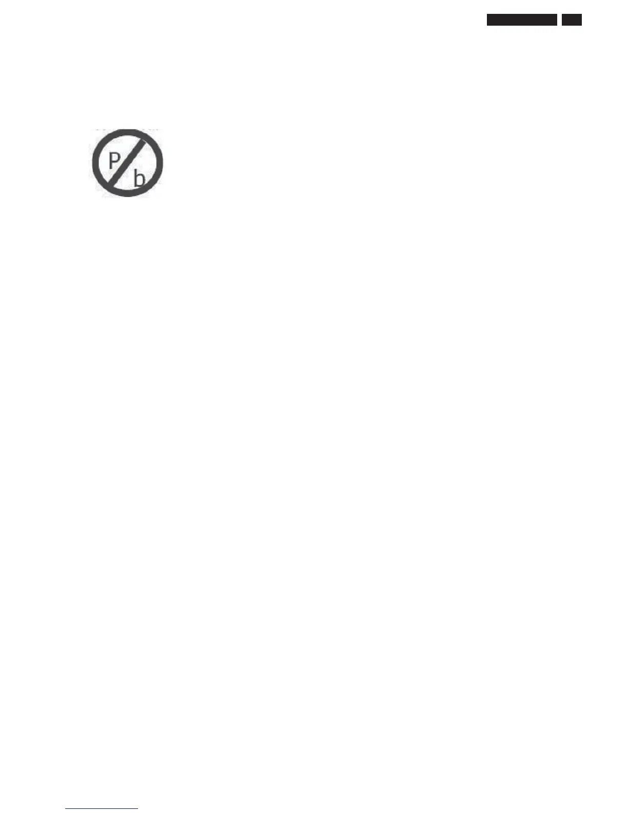
You can identif lead-free product b Philips-lead-free loo on PCB.
4. Lead-free product repair instruction
4.1 Use onl lead-free Solder Allo 0622 149 00106(1.2mm SAC305) or 0622 14900108(1.0mm SAC305).
Remark For lead free solderin material please visit www.alphametals.com
website for details. This is recommended b Philips.
4.2 Use onl adeuate solder tools applicable for lead-free solderin-tin. The solder tool must be able to reach at least a solder-temperature of 400 to
stabilie the adusted temperature at the solder-tip and to echane solder-tips for different applications.
Small Passives/Actives to be removed with thermal tweeers
Automated sstem for IC and BGA repair (Microscope Camera Beam split optics Computer Prorammer Heat controllers Vacuum sstem Laser
pointer) Solder Hand-Tool (Adustable in temperature heiht Temperature shall be held constant Fleible tips)
4.3 Adust our solder tool so that a temperature around 360 -380 is reached and stabilied at the solder oint.
Heatin-time of the solder-oint should not eceed 4 sec. Avoid temperatures above 400 otherwise wear-out of tips will rise drasticall and flu-fluid will
be destroed. Corrosion of Tool-Spikes can be avoided when usin SAC305 and a temperature of less than 400.
4.4 Mi of lead-free solder-tin/parts with leaded solderin-tin/parts is possible but not recommended. If not to avoid clean carefull the solder-oint from old
tin and re-solder with new tin.
4.5 Use onl oriinal spare-parts listed in the Service-Manuals. Standard-material (consumables) can also be purchased at eternal companies.
4.6 Special information for lead-free BGA-ICs this ICs will be delivered in so-called dr-packain to protect the IC aainst moisture and with lead-free
loo on it. This packain ma onl be opened shortl before it is used (soldered). Otherwise the bod of the IC ets wet inside and durin the heatin
time the structure of the IC will be destroed due to hih (steam-) pressure. If the packain was opened before usae the IC has to be heated up for
some hours (around 90 ) for drin (Take attention for ESD-protection)
5. Rework on BGA (Ball Grid Arra) ICs
General
Althouh (LF)BGA assembl ields are ver hih there ma still be a reuirement for component rework. B rework we mean the process of removin
the component from the PWB and replacin it with a new component. If an (LF) BGA is removed from a P WB the solder balls of the component are
deformed drasticall so the removed (LF)BGA has to be discarded.
Device Removal
As is the case with an component that it is essential when removin an (LF) BGA the board tracks solder lands or surroundin components are not
damaed. To remove an (LF)BGA the board must be uniforml heated to a temperature close to the reflow solderin temperature. A uniform temperature
reduces the chance of warpin the PWB.
To do this we recommend that the board is heated until it is certain that all the oints are molten. Then carefull pull the c
omponent off the board with a
vacuum nole. For the appropriate temperature profiles see the IC data sheet.
Area Preparation
When the component has been removed the vacant IC area must be cleaned before replacin the (LF) BGA. Removin an IC often leaves varin
amounts of solder on the mountin lands. This ecessive solder can be removed with either a solder sucker or solder wick. The remainin flu can be
removed with a brush and cleanin aent. After the board is properl cleaned and inspected appl flu on the solder lands and on the connection balls of
the (LF)BGA
Note
Do not appl solder paste as this has shown to result in problems durin re-solderin.
Device Replacement
The last step in the repair process is to solder the new component on the board. Ideall the (LF) BGA should be alined under a microscope or
manifin lass. If this is not possible tr to alin the (LF)BGA with an board markers. To reflow the solder appl a temperature profile accordin to
the IC data sheet. So as not to damae neihbourin components it ma be necessar to reduce some temperatures and times.
More Information
For more information on how to handle BGA devices visit this URL http//www.atourservice.ce.philips.com (needs subscription). After loin select
Maaine then o to Workshop Information. Here ou will find Information on how to deal with BGA-ICs.
241%4L3 LC'