Do you have a question about the Philips FW-V537 and is the answer not in the manual?
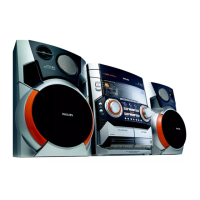
| CD Player | Yes |
|---|---|
| Bluetooth | No |
| USB Playback | Yes |
| FM Radio | Yes |
| Tuner Bands | FM |
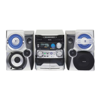
| Number of Discs | 3 |
| Speaker Type | 2-way |
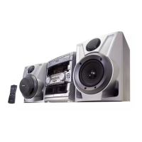
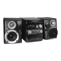
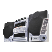
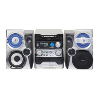
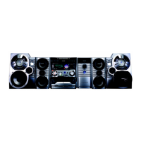
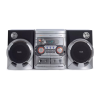
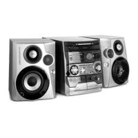
| Type | Mini Hi-Fi System |
Lists features and corresponding board versions.
Technical specifications for the entire system.
FM and MW tuning range, sensitivity, and selectivity specs.
Specifications for the tape deck functions.
Audio and video performance specifications for VCD.
Setup for measuring FM and AM tuner performance.
Setup for measuring CD and tape recorder performance.
Lists necessary tools, cassettes, and ESD protection equipment.
Procedures and precautions for handling surface-mount components.
General safety instructions for repair technicians across multiple languages.
Specific warnings about invisible laser radiation exposure during service.
Identifies system controls and remote control functions.
Steps for inserting batteries and making rear connections.
Connecting antennas and other external audio/video equipment.
Steps for removing the cassette cover and CDC module.
Procedure for separating the MPEG and CDC modules.
Steps for dismantling front boards and the tape module.
Dismantling the rear section and general repair tips.
How to start and navigate the service test program.
Outlines tests for Tuner, Display, VCD, and EEPROM.
Block diagram illustrating the main signal flow.
Diagram showing wiring between main boards and modules.
Diagram showing component placement on the board.
Diagram showing IC and chip placements on the board.
Detailed circuit diagram for the main control board.
Circuit diagram for the IR receiver board.
Circuit diagram for the Key-CDC board.
Circuit diagram for the VU Meter board.
Circuit diagram for the Karaoke board.
List of electronic components for the front control board.
Diagram showing chip placements on the display board.
Diagram showing component placement on the display board.
Detailed circuit diagram for the front display board.
Circuit diagram for the headphone amplifier board.
List of electronic components for the front display board.
Block diagram of the ECO6 Tuner module.
Schematic diagram of the ECO6 Tuner module.
Component layout of the ECO6 Tuner board.
Table for tuning adjustments for different wavebands.
Parts list for miscellaneous items and capacitors.
Parts list for resistors and coils.
Exploded view of the VCD-MPEG-01B module.
Overview of MPEG-01B module operation and communication.
Block diagrams of the MPEG-01B module and microcontroller.
Details of ES3880 chip pins and their functions.
Details of ES3883 chip pins and their functions.
Layout diagram of the MPEG-01B board.
Circuit diagrams for ES3880 and ES3883.
Circuit diagram for the audio amplifier section.
Wiring diagram for the tape deck mechanism.
Block diagram of the ETF7 tape module.
Explanation of playback, recording, dubbing, and mode selection functions.
Details on Dolby circuit, muting, filters, and bias adjustments.
Glossary of terms and abbreviations used in the tape module section.
Connector pin assignments for AF and front board interfaces.
Connector pin assignments for deck control and inter-board communication.
Connector assignments for tape deck control and interface.
Steps for adjusting motor speed, azimuth, and bias levels.
Procedures for checking wow/flutter and frequency response.
Diagram showing component placement on the tape mechanism.
Diagram showing chip placement on the tape mechanism.
Detailed circuit diagram of the analog signal path.
Circuit diagram for the servo control system.
Exploded view of the tape module assembly.
Exploded view of the tape mechanism motor assembly.
List of mechanical parts for tape mechanism A play function.
List of mechanical parts for tape mechanism B Rec/Pb.
List of mechanical parts for tape mechanism B Rec/Pb (autoreverse).
Parts list for miscellaneous items and capacitors.
Parts list for resistors and dial components.
Exploded view showing the parts of the 3CDC-LC module.
Steps for dismantling and assembling the CD tray.
Wiring details and service position of the CD mechanism.
Block diagram showing signal flow between main board and CD mechanism.
Component layout of the 3CDC-LC board from the copperside.
Diagram of components viewed from the copperside.
Circuit diagram for HF amplifier and laser power control.
Table mapping component designators to their locations.
Circuit diagram for signal processor and audio sections.
Circuit diagram for motor control and interface logic.
List of mechanical parts for the 3CDC-LC module.
Overview of the amplifier IC and its operation.
Explanation of the Super Class G amplifier principle.
Details on the standby transformer and power saving.
Explanation of how DC voltages are generated for the amplifier.
Block diagram of the mains power supply board.
Block diagram of the P2001 power amplifier board.
Layout of components on the mains board.
Circuit diagram for the P2001 30-70W mains power supply.
Overview of AF9 board features and IC functions.
Details on MIC MIXING, DPL, LINE OUT, SUB-WOOFER OUT, etc.
Diagram showing component placement on the AF9 board.
Diagram showing chip placement on the AF9 board.
First part of the AF9 board circuit diagram.
Second part of the AF9 board circuit diagram.
Third part of the AF9 board circuit diagram.
List of resistors and coils for the AF9 board.
List of diodes, transistors, and integrated circuits for the AF9 board.
Component and chip layout of the VCD GND Isolator board.
Circuit diagram for the VCD GND Isolator board.
Exploded view of the entire main unit assembly.
List of mechanical parts and accessories for the main unit.
List of screws used in the main unit assembly.