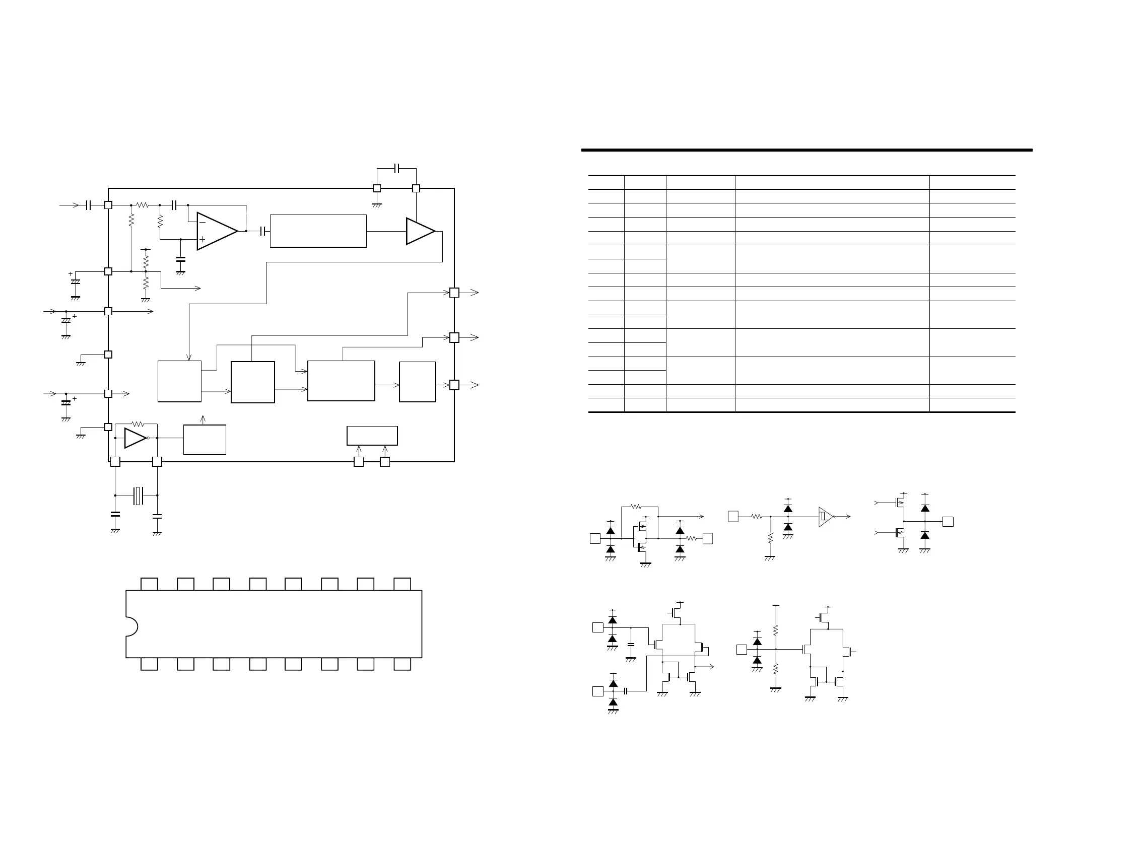
560p
CMP
V
SS3
comparator
8th Switched
capacitor filter
anti-aliasing
filter
100k
120k
100k
270p
MUX
Vref
2.2∝F
V
DD1
1 Analog
Power supply
V
SS1
1
V
DD2
2
Digital
Power supply
V
SS2
XI
XO
4.332MH
Z
33pF
3
33pF
3
PLL
57kH
Z
RDS/ARI
PLL
1187.5Hz
Bi-phase
decoder
Measurement
circuit
Differential
decoder
T1
T2
RDATA
QUAL
RCLK
1: V
DD1
and V
DD2
are separated within the IC.
2: Have V
DD2
(digital power supply) of a sufficiently low impedance.
3: Match the capacitor constants with the crystal manufacturer.
1
2
3
4
5
6
7
8
9
10111213141516
RCLK
(N.C.)
XO
XI
V
DD2
V
SS2
T1
T2
QUAL
RDATA
Vref
MUX
V
DD1
V
SS1
V
SS3
CMP
Reference
clock
(4)
(7) (8)
(3)
(16)
(1)
(2)
(5)
(6)
(12)
(11)
(13) (14) (10) (9)
Pin No. Pin nameSymbol Functions Input/Output type
1 QUAL Demodulator quality Type CGood data: High, bad data : Low
Refer to output data timing
6V
SS1
7
CMP Comparator input Type D
C-junction (refer to input/output circuits )
8
V
SS3 GND
2 RDATA Demodulator data
9T2
Test input Type BOpen or connected to ground
10 T1
3Vref Reference voltage
4 MUX Input
Type E
Type D
1/2 V
DD1 (refer to input/output circuits)
Composite signal input (refer to input/output circuits)
11 V
DD2
Digital power supply
4.5V to 5.5V
12 V
SS2
13 XI
Crystal oscillator Type A
Connects to 4.332MHz oscillator
(refer to input/output circuits)
14 XO
15
(N.C.)
Type C
16 RCLK Demodulator clock 1187.5Hz clock (refer to the timing diagram)
5V
DD1
Analog power supply
4.5V to 5.5V
Type A
Type B
Type D
10M
Type C
Type E
+
+
RDS/RBDS DECODER
BU1923F
RDS/RBDS DECODER
BU1923F
Pins Description
BLOCK DIAGRAM
7-2 7-2