Circuit Diagrams and PWB Layouts
EN 51SDI PDP 7.
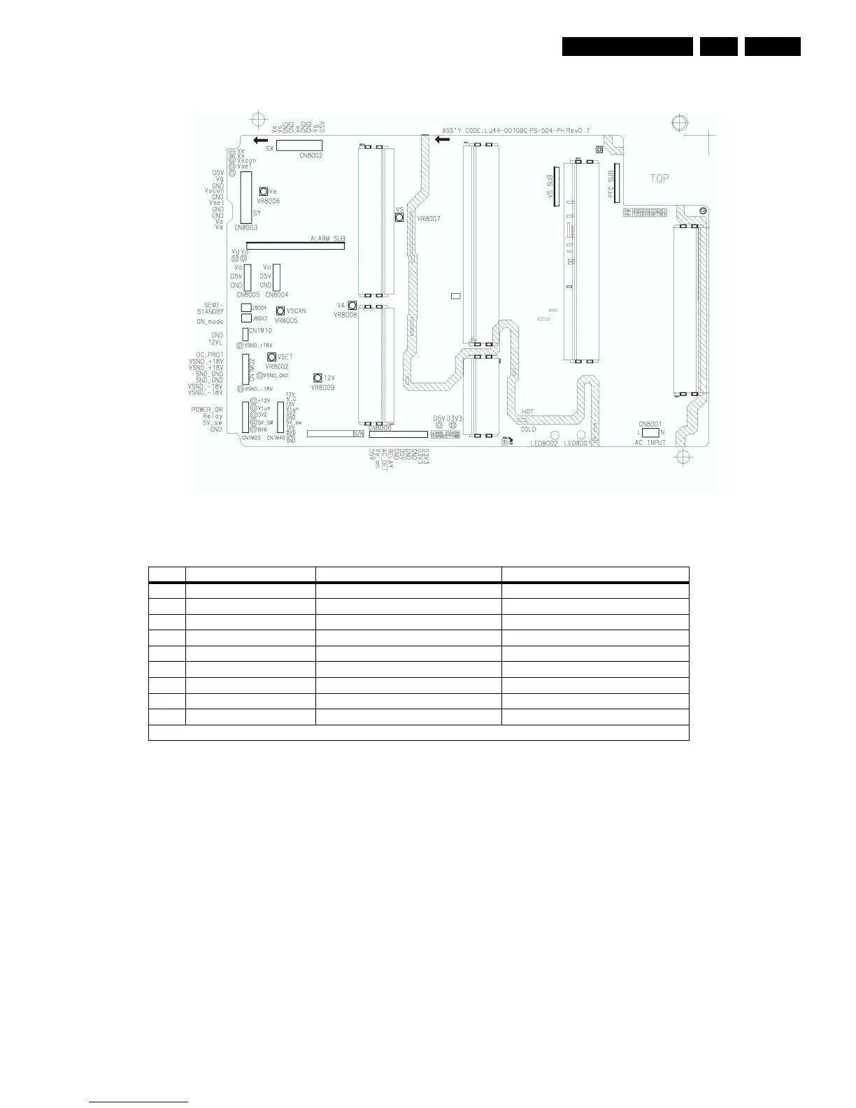
6.2.8 PSU 50" HD v4
Figure 6-16 PSU layout
Table 6-8 Adjustment voltage level overview
7. Circuit Diagrams and PWB Layouts
Not applicable.
F_14991_063.eps
120206
No Output voltage (V) Voltage Setting (Normal Load) Output Voltage Variable Point
1 VS 200V ± 1% 195V ~ 215V
2 VA 70V ± 1.5% 50V ~ 70V
3 VE 100V ± 1.5% 70V ~ 110V
4 VSET 195V ± 1.5% 180V ~ 210V
5 VSCAN -175V ± 1.5% -170V ~ -185V
6 VSB 5V ± 5% Fixed
7 VG 15V ± 5% Fixed
8 D5VL 5.2V ± 5% Fixed
9 D3V3 3.3V ± 5% Fixed
Check voltage label on the PDP for correct values.
 Loading...