Rev. A 10/18
13
Application NoteAN-72
www.power.com
Step 6 – Secondary Components
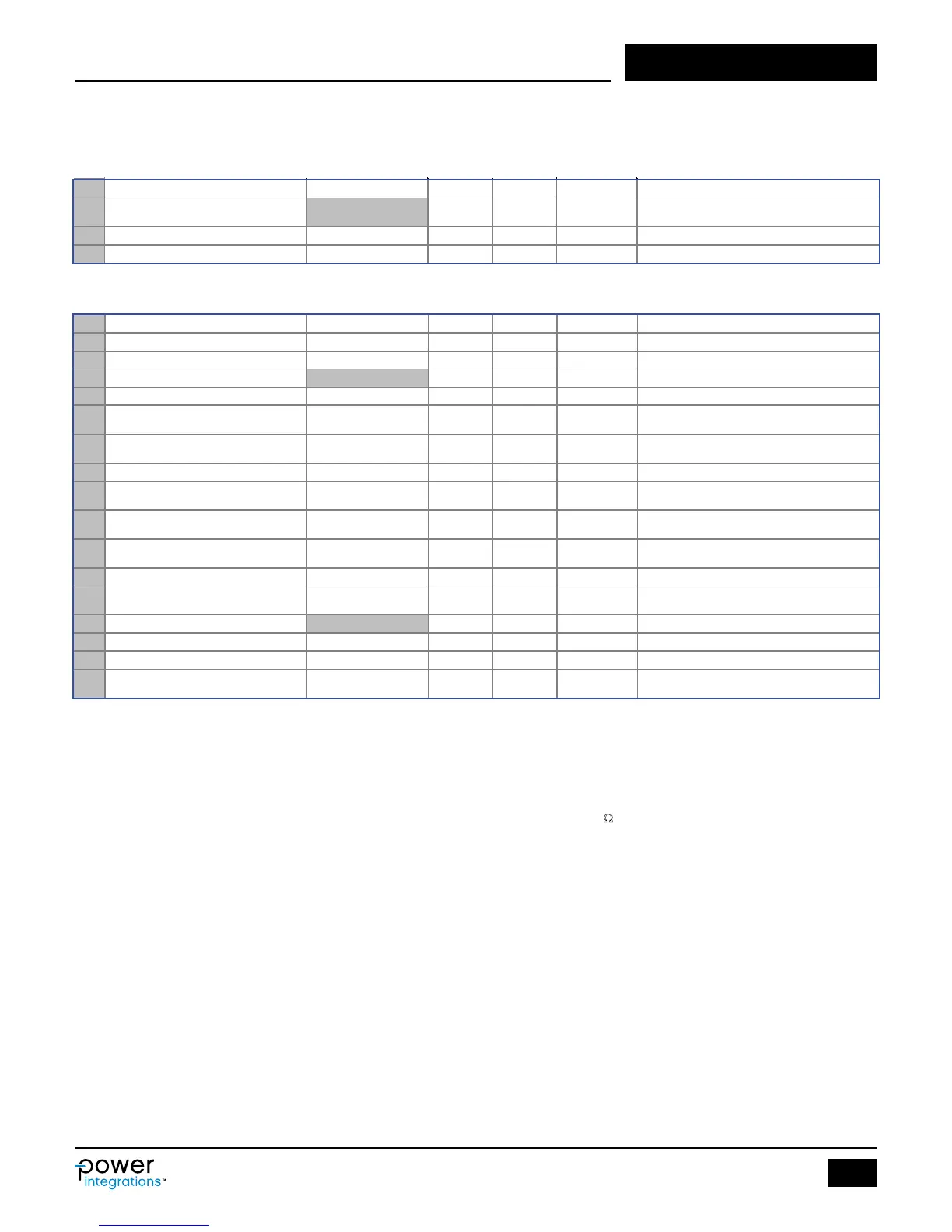
Enter: RFB_UPPER
Figure 9. Secondary Components Section of InnoSwitch3 PIXLs Spreadsheet.
Figure 10. Secondary Components Section of InnoSwitch3 PIXls Spreadsheet.
118
Upper feedback resistor (connected to the first
output voltage)
120 RFB_LOWER 34.00 kΩ Lower feedback resistor
121 CFB_LOWER 330 pF Lower feedback resistor decoupling capacitor
125 MULTIPLE OUTPUT PARAMETERS
126
127 VOUT1 5.00 V Output 1 voltage
128 IOUT1 4.00 A Output 1 current
129 POUT1 20.00 W Output 1 power
130 IRMS_SECONDARY1 5.95 A
Root mean squared value of the secondary
current for output 1
131 IRIPPLE_CAP_OUTPUT1 4.41 A
Current ripple on the secondary waveform for
output 1
132 AWG_SECONDARY1 19 AWG Wire size for output 1
133 OD_SECONDARY1_INSULATED 1.217 mm
Secondary winding wire outer diameter with
insulation for output 1
134 OD_SECONDARY1_BARE 0.912 mm
Secondary winding wire outer diameter without
insulation for output 1
135 CM_SECONDARY1 1191 Cmils
Bare conductor effective area in circular mils for
output 1
136 NSECONDARY1 6 Number of turns for output 1
137 VREVERSE_RECTIFIER1 34.09 V
SRFET reverse voltage (not accounting parasitic
voltage ring) for output 1
138 SRFET1 Auto AON6266 SRFET selection for output 1
139 VF_SRFET1 0.076 V SRFET on-time drain voltage for output 1
140 VBREAKDOWN_SRFET1 60 V SRFET breakdown voltage for output 1
141 RDSON_SRFET1 19.0 mΩ
SRFET on-time drain resistance at 25degC and
VGS=4.4V for output 1
Upper Feedback Resistor, RFB_UPPER
The RFB_UPPER resistor value is calculated based on VOUT and the
nominal internal reference voltage of the IC (1.265 V).
Upper Feedback Resistor, RFB_LOWER
The RFB_LOWER resistor is calculated based on VOUT and the 1.265 V
internal reference voltage. The value will change if the specied
value is used for the RFB_UPPER resistor.
Lower Feedback Resistor Decoupling Capacitor, CFB_LOWER
A 330 pF surface mount ceramic X7R type capacitor (or better) is
recommended as this can be placed close to the pins of the FEEDBACK
and GROUND pins of the IC.
Step 7 – Multiple Output Parameters
This section allows the user to design up to three secondary outputs
(excluding bias supply) and choose a suitable MOSFET size for
synchronous rectication. The spreadsheet will provide a warning
should the total power of the multiple outputs exceed the power
described in the POUT cell.
For single output design, cells VOUT1, IOUT1 and POUT1 will be
the main output parameters entered in section 1.
Each output provides a selection of synchronous rectier MOSFETs
(SRFET) in the drop down menu, (see Table 10). Based on the SR
FET chosen the on-state forward voltage, VF_SRFET (V), breakdown
voltage, VBREAKDOWN_SRFET (V), and on-time drain resistance,
RDSON_SRFET (m
Ω) will be displayed in the spreadsheet.
The spreadsheet also calculates the critical electrical parameters for
each secondary output:
RMS Current of the Secondary Output, RMS_SECONDARY (A)
– Used to size the secondary winding wire.
Current Ripple on Secondary, IRIPPLE_CAP_OUTPUT (A)
– Used to size the output lter capacitor.
–Number of Turns for Output, NSECONDARY
– Calculated turns for each output.
Additional information for the magnetic wire are also given, AWG_
SECONDARY (AWG), OD_SECONDARY_INSULATED (mm) and
OD_SECONDARY_BARE (mm).