NB-IoT Module Series
BC660K-GL Hardware Design
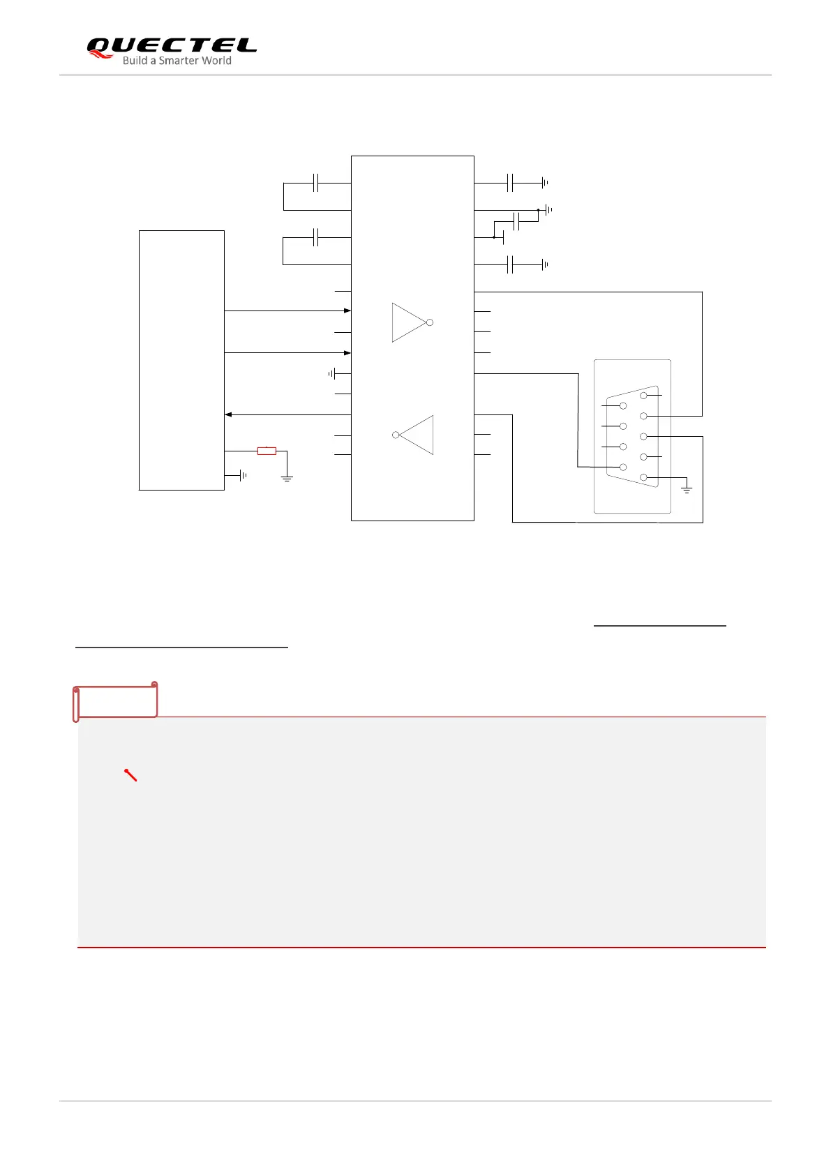
BC660K-GL_Hardware_Design 29 / 57
according to the actual situation.
Figure 14: Reference Design for Module-PC Communication via RS-232 Interface
Please visit vendors’ websites to select a suitable RS-232 transceiver, such as http://www.exar.com and
http://www.maximintegrated.com.
1. If the voltage domain of your application system is 1.8 V, keep the R1 in red not mounted; if it is
3.3 V, keep the R1 in red mounted.
2. “ ” represents the test points of UART interfaces. It is recommended to reserve the test points of
VBAT, BOOT and RESET_N for convenient firmware upgrade and debugging when necessary.
3. MAIN_RXD cannot be pulled up to VDD_EXT directly. To pull up MAIN_RXD to VDD_EXT, you
need to connect a Schottky diode in series first, and then add a pull-up resistor of 4.7–20 kΩ. For
more details, see document [3].
4.
1)
When VIO_SEL is grounded and VBAT ˂ 3.3 V, VDD_EXT = VBAT;
When VIO_SEL is grounded and VBAT ≥ 3.3 V, VDD_EXT = 3.3 V;
When VIO_SEL is floating, VDD_EXT = 1.8 V.
When the serial port voltage is neither 1.8 V nor 3.3 V, it is recommended to use a level conversion circuit.
For the design of the circuit shown in the dotted line, refer to that shown in the solid lines, and pay
attention to the connection direction. In this case, the design of RI – GPIO circuit can refer to that of the
MAIN_TXD – RXD circuit.