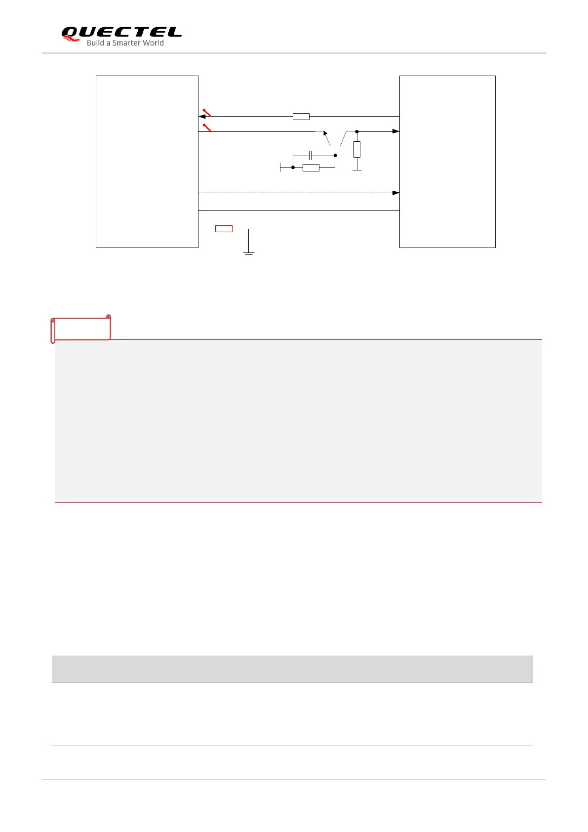
1. Due to the anti-backflow design of the MAIN_RXD pin, it can be directly connected to the TXD of
DTE in 1.8–3.3 V voltage domain. If wake-up function of MAIN_RXD in Deep Sleep/Light Sleep
mode is enabled, it is recommended that MAIN_RXD not use any level conversion circuit so as to
avoid abnormal wake-up.
2. If you apply the level conversion circuit, don’t mount the R1 marked in red.
3. MAIN_RXD cannot be pulled up to VDD_EXT directly. To pull up MAIN_RXD to VDD_EXT, you
need to connect a Schottky diode in series first, and then add a pull-up resistor of 4.7–20 kΩ. For
more details, see document [3].
4. The level conversion circuit does not apply to applications with high baud rates exceeding
460 kbps.
3.8. USIM Interface
The USIM card is powered by USIM_VDD. Both 1.8 V and 3.0 V USIM cards are supported.
Table 12: Pin Definition of USIM Interface
When 3.0 V ≤ VBAT ≤ 4.3 V, support
1.8/3.0 V USIM card;
When 2.2 V ≤ VBAT < 3 V, only support
1.8 V USIM card;