NB-IoT Module Series
BC660K-GL Hardware Design
BC660K-GL_Hardware_Design 37 / 57
4.4. Reference Design of RF Layout
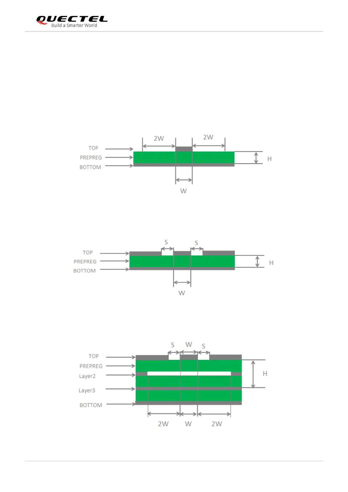
The characteristic impedance of all RF traces on your PCB should be controlled at 50 Ω. The impedance
of the RF traces is usually determined by the trace width (W), the material’s dielectric constant, the height
from the reference ground to the signal layer (H), and the clearance between RF traces and grounds (S).
The microstrip or coplanar waveguide is typically used in RF layout to control characteristic impedance.
The following are reference designs for microstrip or coplanar waveguide transmission lines with different
PCB structures.
.
Figure 20: Microstrip on a 2-layer PCB
Figure 21: Coplanar Waveguide on a 2-layer PCB
Figure 22: Coplanar Waveguide on a 4-layer PCB (Layer 3 as Reference Ground)