Wi-Fi Module Series
FGH100M_Hardware_Design 20 / 41
4.4. Wi-Fi Application Interface
The module provides SDIO 2.0 interface for Wi-Fi function. If power saving mode is used, a GPIO of the
host is needed to be set as a CMOS input pin to receive the BUSY signal from the pin 10 (GPIO0) of the
module. If needed, please contact Quectel Technical Support.
4.4.1. SDIO Interface
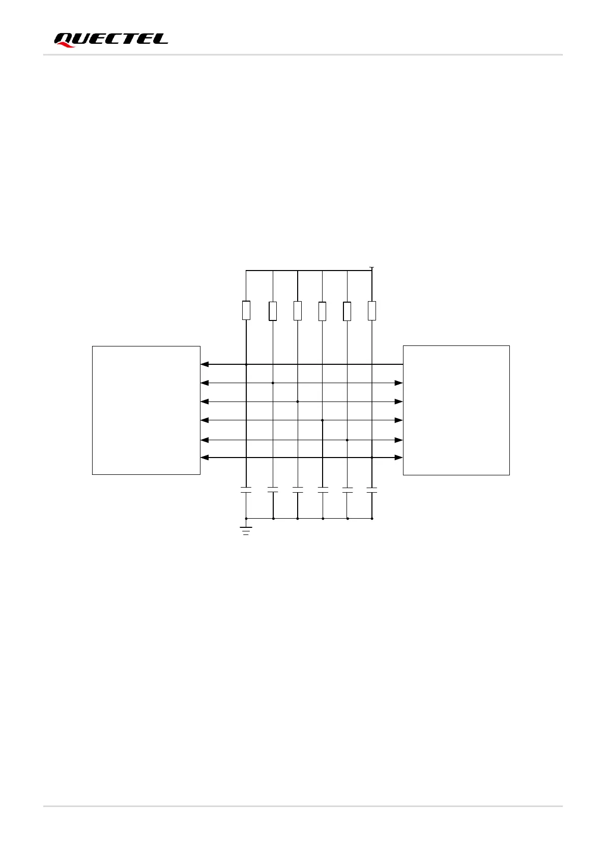
SDIO interface connection between the module and the host is illustrated in the following figure.
SDIO_CLK
SDIO_CMD
SDIO_DATA0
SDIO_DATA1
SDIO_DATA2
SDIO_DATA3
Host
Module
SDIO_DATA0
SDIO_DATA1
SDIO_DATA2
SDIO_DATA3
SDIO_CLK
SDIO_CMD
NM_10K
VDDIO
NM_10K
NM_10K
NM_10K
NM_10K
NM NM NM NM NM NM
NM_10K
Figure 4: SDIO Interface Connection
To ensure compliance of interface design with the SDIO 2.0 specification, it is recommended to adopt the
following principles:
⚫ To avoid jitter of bus, pull up SDIO_CMD and SDIO_DATA_[0:3]/SDIO_CMD to VDDIO with resistors
respectively. Value range of these resistors should be 10–100 kΩ and the recommended value is
10 kΩ.
⚫ The impedance of SDIO signal traces is 50 Ω ±10 %. Route the SDIO traces in inner layer of the PCB,
and surround the traces with ground on that layer and with ground planes above and below.
⚫ Keep SDIO signals far away from other sensitive circuits/signals such as RF circuits and analog
signals, as well as noise signals such as clock signals and DC-DC signals.
⚫ The distance between SDIO signals and other signals must be greater than twice the trace width, and
the bus load capacitance must be less than 15 pF.