Wi-Fi Module Series
FGH100M_Hardware_Design 22 / 41
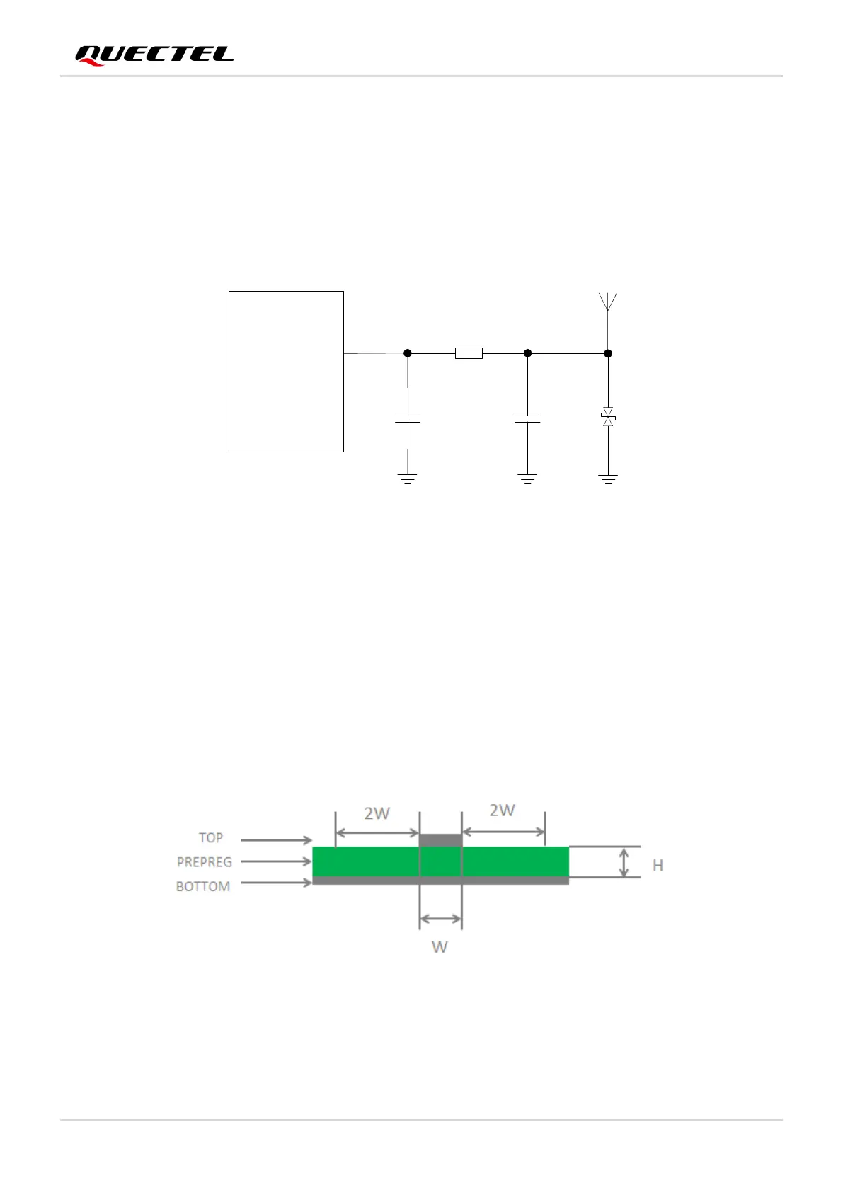
4.6.1. Reference Design
A reference circuit for the RF antenna interface is shown below. It is recommended to reserve a π-type
matching circuit and add ESD protection components for better RF performance. Reserved matching
components (R1, C1, C2, and D1) shall be placed as close to the antenna as possible. C1, C2 and D1 are
not mounted by default. The parasitic capacitance of TVS should be less than 0.05 pF and R1 is
recommended to be 0 Ω.
Figure 5: Reference Circuit for RF Antenna Interface
4.6.2. RF Routing Guidelines
For user’s PCB, the characteristic impedance of all RF traces should be controlled to 50 Ω. The
impedance of the RF traces is usually determined by the trace width (W), the materials’ dielectric constant,
the height from the reference ground to the signal layer (H), and the spacing between RF traces and
grounds (S). Microstrip or coplanar waveguide is typically used in RF layout to control characteristic
impedance. The following are reference designs of microstrip or coplanar waveguide with different PCB
structures.
Figure 6: Microstrip Design on a 2-layer PCB