GNSS Module Series
LC76G_Series_EVB_User_Guide 15 / 33
Test Point No. Test Point Label Test Point Function I/O Description
23 16 U103: Pin 16 DIO I2C_SDA: I2C serial data
24 14 U103: Pin 14 PO
external RF components
25 12 GND - Ground
26 10 GND - Ground
27 8 U103: Pin 8 PI VCC: Main power supply
28 6 U103: Pin 6 PI
V_BCKP: Backup power supply
for backup domain of module
29 4 U103: Pin 4 DO 1PPS: 1 pulse per second
30 PIN2 U103: Pin 2 DO TXD: Transmits data
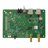
1. Test points of J402 are arranged clockwise, and their serial numbers are shown in Figure 3: EVB
Top View.
2. A J402 test point refers to the module’s corresponding function. For detailed descriptions, see
document [1] hardware design.
 Loading...