HSPA/UMTS/GSM/GPRS Module Series
UG96&UG95&M95 R2.0 Compatible Design
UG96&UG95&M95 R2.0_Compatible_Design 27 / 42
1. UG96/UG95’s UART pins belong to 1.8V power domain.
2. M95 R2.0’s UART pins belong to 2.8V power domain.
3. It is recommended to reserve USB_DP, USB_DM and USB_VBUS pins as test points and then place
them on DTE for debugging.
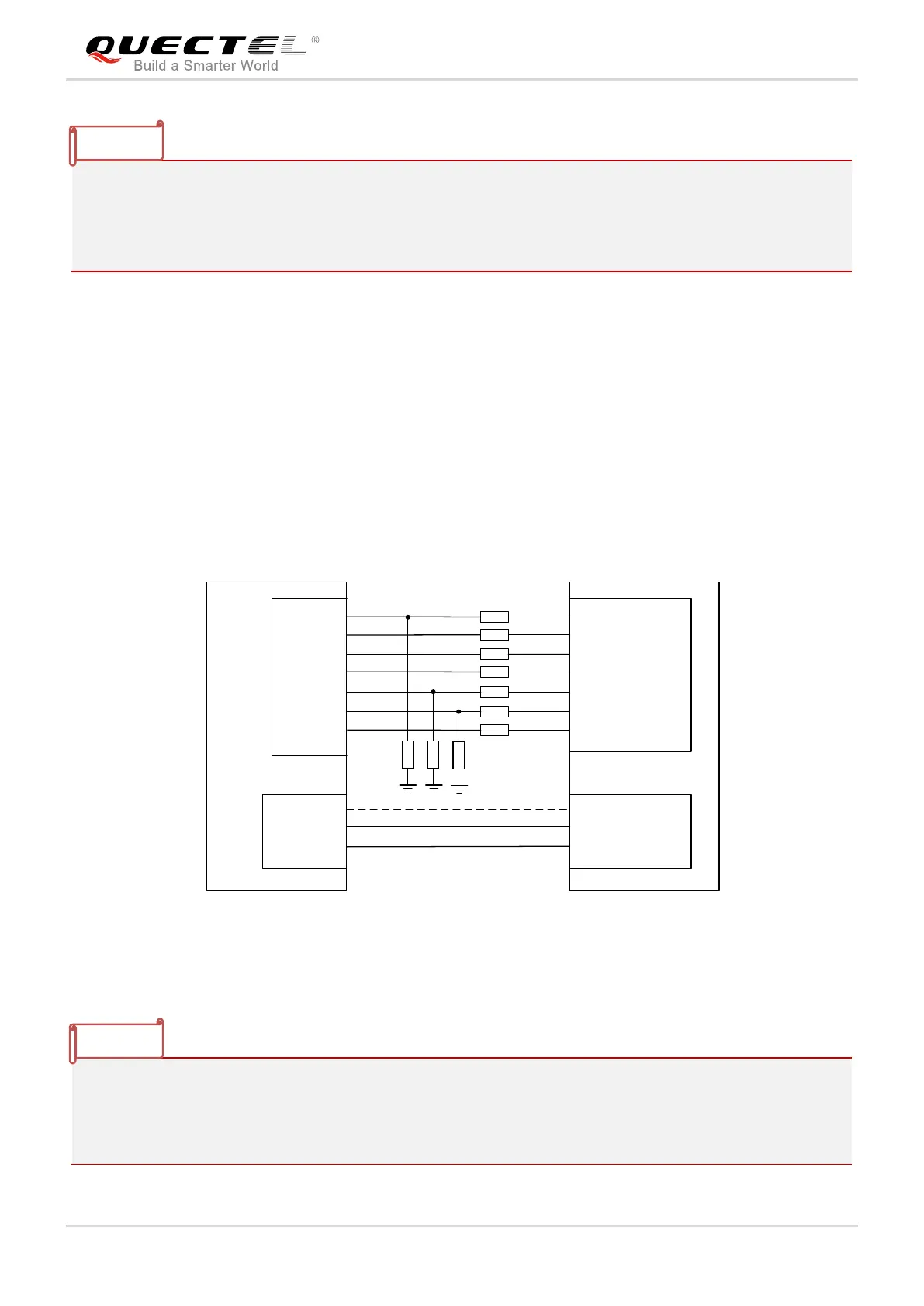
4.8. USB Interface
UG96/UG95 provides one integrated Universal Serial Bus (USB) interface, which complies with the USB
2.0 specifications and supports high speed (480Mbps) and full speed (12Mbps) modes on USB 2.0. It
supports USB device only.
If application processor communicates with UG96/UG95 via USB interface and communicates with M95
R2.0 via UART interface, the reference design for UG96/UG95’s USB interface and M95 R2.0’s main
UART interface is shown as the following figure.
DCD
RTS
DTR
RXD
RI
CTS
TXD
Module
USB_VBUS
USB_DP
USB_DM
UART
USB
Processor
DCD
RTS
DTR
RXD
RI
CTS
TXD
USB_VBUS
USB_DP
USB_DM
M95
R2.0
UG96/
1K
1K
1K
1K
1K
1K
1K
UG95
5.6K5.6K5.6K
R1 R2 R3
Figure 16: Reference Design of USB Interface (UG96/UG95) and UART Interface (M95 R2.0)
1. The resistance 5.6K is used on 3.3V IO level system. While on 3V IO level system, the resistance of
R1~R3 should be changed to 10KΩ, and the max input voltage to module should be 2.8V.
2. Please pay attention to the voltage level matching between the module and processor. For details,
please refer to document [4].