1
and 2.
Pin
3 of
Z41 will
go
low
causing current to flow
through relay K1's
coil. K1's
contacts close, shorting
out
pins 1 and 3 of
J3.
These
two pins are
associated
with the
remote jack at
the recorder.
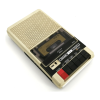
The recorder's motor
will
then
turn on.
Notice diode
CR3
and
Zeners
CR9
and
CR10. CR3
is
a
standard
silicon diode used for
an "anti-chatter"
function.
When power
is applied or
removed from K1's
coil, a
counter
EMF
is
generated.
This voltage could be
high
enough
to
damage
Z41's output
transistor, or cause K1
to
click off and on a
couple of
times producing undue wear
to
the switching
contacts.
CR3 will shunt the counter
EMF
voltage around K1
and prevent
transistor damage or
relay
chatter. Zener diodes CR9 and CR10
are used in somewhat
the
same
way.
Here
we're trying to
protect
KTs
switch
contacts. When the
recorder
is
turned
on, a high
voltage
spike could
be
produced.
It could
be deadly
-
the contacts
could
weld together
because of a
high
voltage arc.
CR6 and
CR10 prevent
possible
damage by
shunting any
voltage
spikes
above
a
certain
level away
from the contacts.
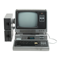
CASSETTE
AUDIO OUTPUT
After the motor
is turned on, the
CPU
may output data for
storage
on tape.
All
data
timing for this output
function is
software
controlled.
Z59
is
used to store data from the
CPU
and it
"builds" the
output
waveform
using
CPU data.
CPU
data,
under software
control, is applied to
latch Z59 on
pins
4
and
5. Output pins 2
and 6 are
connected
to a
resis-
tor
network consisting
of R53 through R56. As
OUTSIG*
is clocking data into
Z59, the
resulting output on the line
labeled CASSOUT,
resembles
a
sine wave built out of square
waves.
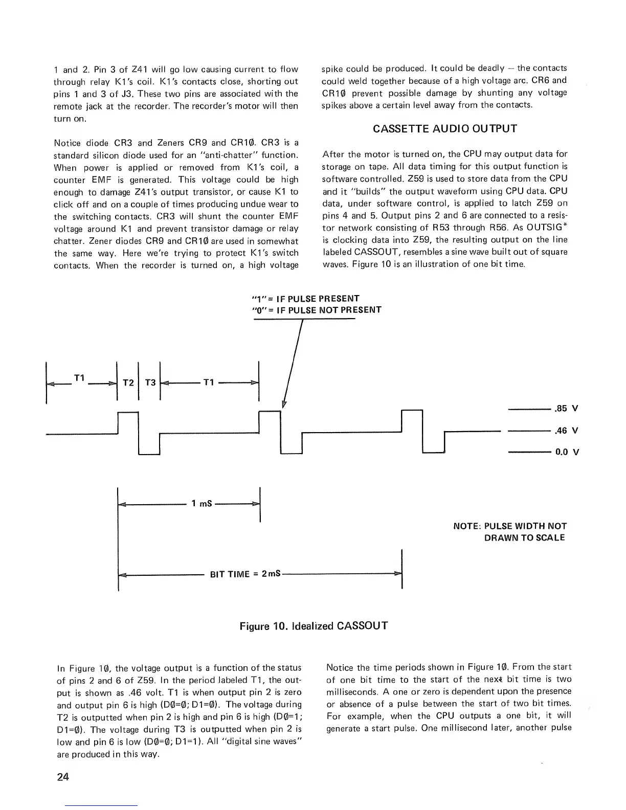
Figure 10 is an illustration of one
bit time.
"1"=
IF
PULSE
PRESENT
"0"=
IF PULSE
NOT
PRESENT
.85 V
.46 V
0.0
V
1
mS
NOTE:
PULSE WIDTH NOT
DRAWN
TO
SCALE
BIT TIME
=
2mS-
Figure
10.
Idealized
CASSOUT
In Figure
10,
the
voltage
output is a
function
of
the status
of pins 2 and 6
of
Z59. In the
period .labeled
T1, the out-
put is shown
as .46
volt. T1 is
when output pin 2
is zero
and
output pin
6 is high
(D0=0; D1=0).
The voltage
during
T2
is outputted
when pin
2 is high and
pin
6
is high
(D0=1
;
D1=0).
The
voltage during
T3 is
outputted when
pin
2
is
low
and pin 6 is
low (D0=0;
D1=1).
All
"digital
sine
waves"
are
produced in
this way.
Notice the time
periods
shown in
Figure
10.
From the start
of
one bit time
to the
start of
the nex* bit
time is two
milliseconds.
A one or
zero is
dependent
upon the
presence
or
absence of a
pulse
between the
start of two
bit times.
For
example, when
the
CPU outputs a
one
bit, it will
generate a start
pulse. One
millisecond
later,
another pulse
24
 Loading...