After rectification,
the signal
is inverted
and amplified.
Z4,
pins
8,
13 and
9,
is
wired
to form an
inverting amplifier
circuit. The
ratio
of R41
to
R42 gives
the amplifier a
gain
of about
2. Line
C in Figure 4
shows a typical output at
Z4,
pin 9.
The last stage of Z4 is used as
a
level detector. CR6 and
CR7, together with C39, form
a power supply of sorts.
The
amplified audio signal from Z4,
pin
9,
is applied
to
the
anode of CR6. CR6 and CR7 decrease
the voltage level of
the incoming signal by about
.8 to 1.0 volt. C39 filters the
resulting voltage
and creates a
DC
signal like the one shown
on
line D
of
Figure
1 1.
If
the signal output from
Z4,
pin
9,
drops
below
the reference voltage
level
at
C39,
Z4,
pin
10,
will
go
low. It will
stay
low
as long as the voltage on pin
1 2 of
Z4
stays below the reference. Line
E
shows the result-
ing output from Z4, pin 10. Notice that we
lost a
couple of
pulses of audio because the signal did not swing
toward
ground enough
to
trigger Z4, pin
10.
The
negative transac-
tion at pin 10
will
be used to set
flip-flop Z24.
Cassette
data
will
be converted
into
program data by the software
in ROM and
the CPU.
INSIG*
Exactly
how
the
CPU
turns a string of ones and zeroes
into the text of a basic program would interest only the
hardcore
software
person. The
amount
of
hardware used in
the
TRS-80
to get
cassette
data to the
CPU
is
minimal.
Only
the hardware
will
be
discussed.
Z25,
pin
4,
is tied to
IN*.
This signal will go low when
the
CPU
wants to
input data from
a port.
Port
addressing has
already been
discussed. A low
at
pin 4
of Z25 and a low at
address decoder Z36, pin
3,
will cause a low at Z25,
pin
6,
INSIG*. This signal is controlling only
one
device
—
part of
Z44.
Z44, pin
12,
is
tied
to pin 8 of
NAND
gate Z24. The
two
NAND
gates
of Z24 are wired
to
form
a
set-reset
latch.
If
pin 9 goes low,
pin
8
will
go
high.
Pin
8
is cross tied to
pin 12. If pin 13 is
high and since 12 is high, pin 1 1 will be
low. With a high at pin 8
and a low
at
pin
11,
the flip-flop
is said
to
be
set.
If pin 8 is low and pin
1
1 is high, the flip-
flop is reset. The flip-flop is being set by cassette data and
reset by
OUTSIG*. Z44 monitors the status of Z24 under
command from INSIG*.
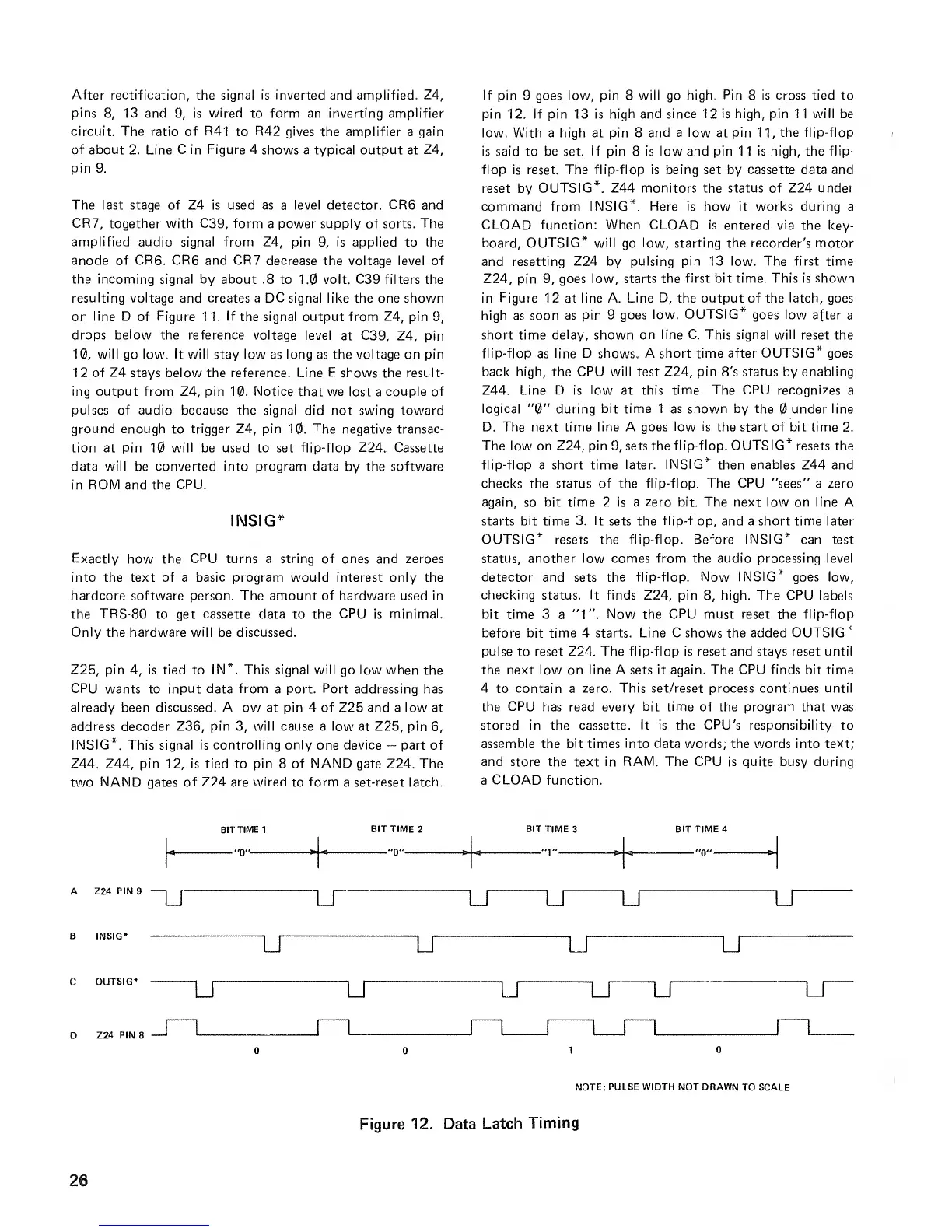
Here is
how it works during a
CLOAD function: When CLOAD is
entered via the key-
board, OUTSIG* will
go
low, starting the recorder's motor
and
resetting Z24 by pulsing pin 13 low. The first time
Z24,
pin
9,
goes low,
starts the first bit time. This is
shown
in
Figure
1 2 at line A.
Line D,
the output of the
latch,
goes
high as
soon as pin
9 goes
low. OUTSIG*
goes
low
after a
short time
delay,
shown
on line C. This signal will
reset the
flip-flop
as
line D shows. A short time after OUTSIG* goes
back high, the
CPU
will test
Z24,
pin 8's status by enabling
Z44. Line D is
low
at this
time. The CPU recognizes
a
logical
"0"
during
bit time 1 as shown by the
under
line
D. The next time line A goes
low is
the start of bit time
2.
The
low on
Z24,
pin
9,
sets the
flip-flop. OUTSIG*
resets the
flip-flop a short time
later. INSIG*
then
enables
Z44 and
checks the status of the flip-flop.
The CPU
"sees" a zero
again,
so
bit time 2 is a zero bit. The next low on line A
starts
bit
time
3. It
sets the
flip-flop,
and a short time later
OUTSIG* resets the flip-flop. Before
INSIG*
can test
status, another low comes from the audio processing level
detector and
sets the
flip-flop. Now
INSIG*
goes low,
checking
status.
It
finds Z24, pin
8,
high.
The CPU labels
bit time 3
a
"1".
Now the
CPU
must reset the flip-flop
before bit time 4 starts. Line C shows the added OUTSIG*
pulse
to
reset Z24. The flip-flop is reset and stays reset until
the next low on line A sets it again. The
CPU finds
bit time
4
to
contain
a
zero. This set/reset process continues until
the CPU
has read every
bit time
of the
program
that was
stored in the cassette. It is the
CPU's
responsibility
to
assemble
the
bit
times
into data
words; the
words
into
text;
and store the
text
in RAM. The
CPU
is quite busy during
a
CLOAD
function.
BIT
TIME
1
BIT TIME
2
"0"
g»j*q
"Q"~
BIT TIME
3
"1"
BIT TIME
4
-0"
A
Z24 PIN
9
"U"
i_r
is u u u
B
INSIG"
i_r u u u
C
OUTSIG*
u
u U U LI
i_r
D
Z24 PIN 8
_J
NOTE: PULSE WIDTH NOT DRAWN
TO SCALE
Figure 12. Data
Latch
Timing
26
 Loading...