SYSTEM POWER
SUPPLY
+12
V POWER
SUPPLY
The
TRS-80 needs three voltage levels: +12
volts
at about
350
milliamps; +5
volts at about
1.2 amps; and
—5
volts
at 1 milliamp.
The
+12
and
—5
volts
are
needed by system
RAM and everything needs +5 volts.
The +12
volt and
+5
volt supplies are regulated
and current protected
against
shorts. The
—5
volts supply
is not as critical
as the other
two supplies, and
it uses a
single zener
diode for
regulation.
Raw, unregulated
power
is supplied
to
all
regulator cir-
cuits from
a
UL approved
"AC adapter."
AC ADAPTER
The AC adapter
(or power
pack)
is a large version of the
type used in calculators or TV game products. Inside the
plastic case is
a
single transformer
with one primary and
two
secondary
windings.
The
primary circuit is designed for
115
VAC
and has an operating range of 105 to 135 VAC.
There
is a wire fuse in the primary side to meet UL speci-
fications.
The two secondary circuits
are both center tapped. One
secondary is rated
at
14 volts AC
at 1
amp. This circuit is
used in the
+5
and
—5
volt supplies. The other secondary
winding uses internal
diodes
and it outputs 19.8
VDC
at
about 350 milliamps. This circuit is used in generating the
12 volt supply.
All voltage outputs
and center taps are
brought into the
power input at J1.
Raw,
unregulated voltage
for the +12V supply
is inputted
at pin
2 of
J1.
When
power switch S1 is closed, C8 filters
the voltage and the
net result is 20 volts,
or so, applied to
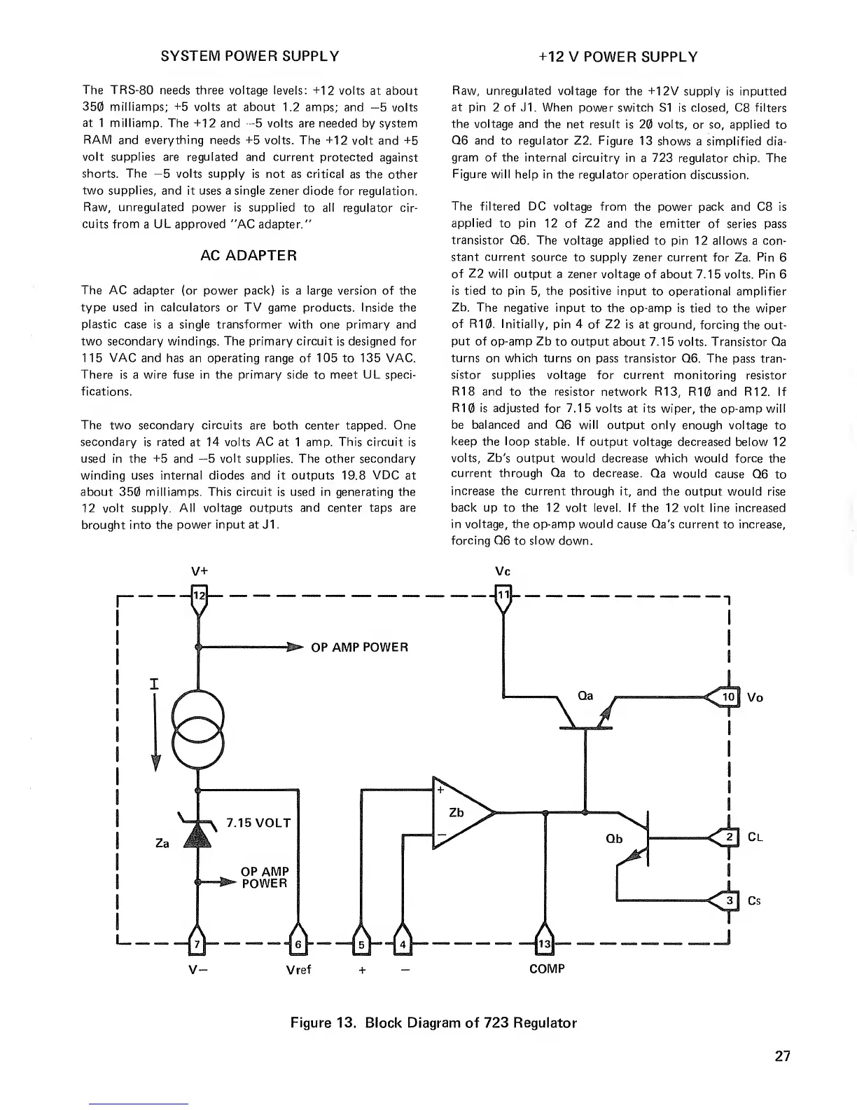
Q6 and to regulator Z2. Figure
13 shows
a simplified dia-
gram of the internal circuitry
in
a
723
regulator chip. The
Figure
will help in
the regulator
operation discussion.
The
filtered DC voltage from
the power pack and C8 is
applied
to pin 12
of
Z2
and the emitter of series
pass
transistor
Q6. The voltage applied
to pin 12 allows a con-
stant current source
to supply
zener
current for Za. Pin
6
of
Z2
will output
a
zener
voltage of about 7.15 volts. Pin
6
is tied
to pin
5,
the positive input
to operational amplifier
Zb. The
negative input
to the op-amp is tied
to
the wiper
of R10. Initially,
pin 4 of Z2 is
at ground,
forcing the
out-
put of op-amp Zb
to output about 7.15 volts. Transistor
Qa
turns on which turns
on pass transistor Q6. The
pass tran-
sistor supplies voltage
for current monitoring resistor
R18 and to the resistor
network
R13,
R10 and R12. If
R10 is
adjusted for 7.15 volts
at
its
wiper, the op-amp
will
be balanced and Q6 will
output only enough voltage to
keep the loop
stable.
If
output voltage
decreased below 12
volts,
Zb's output
would decrease which would force the
current through Qa to decrease.
Qa would cause
Q6
to
increase
the
current
through it,
and
the
output would rise
back
up to the 12 volt level. If
the 12 volt line increased
in voltage, the op-amp would
cause Qa's current to increase,
forcing Q6
to
slow
down.
Vc
OP AMP
POWER
V-
\Qa
y-
Qb
—
—4
7
1—
—
—
—
—
»
J
5
I-
—
—4
g
j—•
«J
4
J—
—
—
—
—
—
•
—
41
31—
•
-—
<2°1
Vo
I
1
4
Cl
Cs
._J
V- Vref
COMP
Figure 13. Block Diagram of 723 Regulator
27

 Loading...