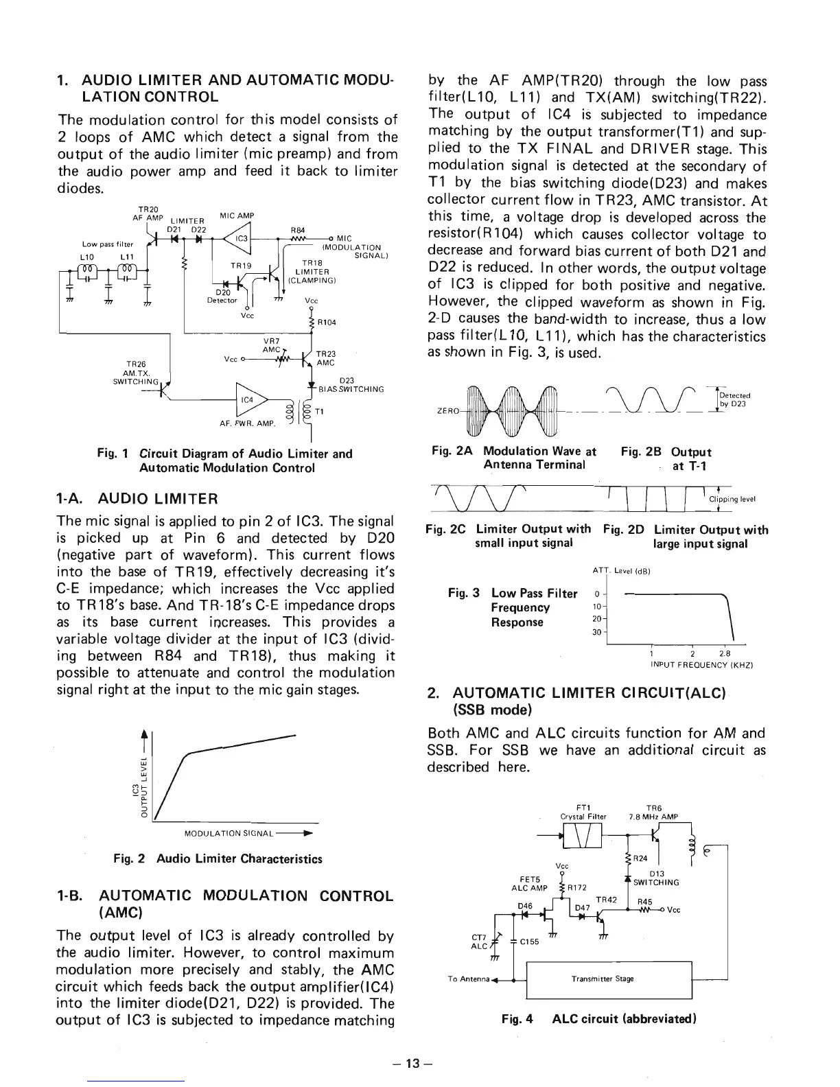
1.
AUDIO
LIMITER
AND
AUTOMATIC
MODU-
LATION
CONTROL
The modu lation control
for
th
is
model consists
of
2 loops
of
AMC which detect a signal
from
the
output
of
the audio
limiter
(mic preamp) and
from
the audio power amp
and
feed
it
back
to
limiter
diodes.
TR20
AF AMP
LIMITER
Low
pass
filter
r
TR26
AM.TX.
021
022
MIC AMP
R84
I--~~'-----o
MIC
Vee
(MODULATION
SIGNAl)
TR18
LIMITER
(CLAMPING)
Vee
R104
TR23
AMC
SWITCHING
023
BIAS SWITCHING
~I
AF.
PWR.
AMP.
Fig. 1 Circuit Diagram
of
Audio Limiter and
Automatic
Modulation Control
1-A.
AUDIO
LIMITER
The mic signal
is
applied
to
pin 2
of
IC3. The signal
is
picked up at Pin 6 and detected
by
D20
(negative
part
of
waveform). This current flows
into
the
base
of
TR 19, effectively decreasing it's
C-E
impedance; which increases the Vcc applied
to
TR 18's
base.
And TR-18's
C-E
impedance drops
as
its
base
current increases. This provides a
variable voltage divider at the
input
of
I
C3
(divid-
ing between R84 and
TR
18), thus making
it
possible
to
attenuate
and
control the modulation
signal right at the
input
to
the mic gain
stages.
t
w
>
W
...J
Mf-
U::J
-0..
f-
::J
o
MODULATION
SIGNAL---.
Fig. 2 Audio Limiter Characteristics
1-8.
AUTOMATIC
MODULATION
CONTROL
(AMC)
The
output
level
of
IC3
is
already controlled
by
the audio limiter. However,
to
control
maximum
modulation more precisely and stably, the AMC
circuit
which feeds back the
output
amplifier(lC4)
into
the
limiter
diode(D21, D22)
is
provided. The
output
of
IC3
is
subjected
to
impedance matching
by the
AF
AMP(TR20) through the low
pass
filter(
L 10, L 11) and
TX(AM)
switching(TR22).
The
output
of
IC4
is
subjected
to
impedance
matching by the
output
transformer(T1)
and
sup-
plied
to
the
TX
FINAL
and
DRIVER
stage.
This
modulation signal
is
detected at the secondary
of
T1
by
the bias switching diode(D23)
and
makes
collector current
flow
in TR23, AMC transistor.
At
this time, a voltage drop
is
developed
across
the
resistor( R 1 04) wh ich
causes
collector voltage
to
decrease
and
forward bias current
of
both
D21
and
D22
is
reduced. I n other words, the
output
voltage
of
I
C3
is
cl
ipped
for
both
positive
and
negative.
However, the
cl
ipped waveform
as
shown in Fig.
2-D
causes
the band-width
to
increase, thus a
low
pass
fi
Iter( L 10, L 11), wh ich
has
the characteristics
as
shown in Fig. 3,
is
used.
-tH-
~
-
J
Detected
ZERO _
__
__
_ _ _
by
023
Fig.2A
Modulation
Wave
at
Antenna
Terminal
Fig.
26
Output
at
T-1
\ I \ I I
c+Pin
g
level
Fig. 2C Limiter
Output
with Fig. 2D Limiter
Output
with
small
input
signal large
input
signal
Fig. 3 Low Pass Filter
Frequency
Response
ATT.
Level (dB)
o
10
20
30
1 2.8
INPUT FREQUENCY
(KHZ)
2.
AUTOMATIC
LIMITER
CIRCUIT(ALC)
(SSB mode)
Both AMC and
ALC
circuits
function
for
AM
and
SSB.
For
SSB
we
have
an
additional
circuit
as
described here.
CT7
ALC
FT1
TR6
Crystal Filter 7.8 MHz AMP
013
SWITCHING
R45
.
~----Mr---o
Vee
To Antenna Transmitter
Stage
Fig. 4 ALC
circuit
(abbreviated)
-13
-