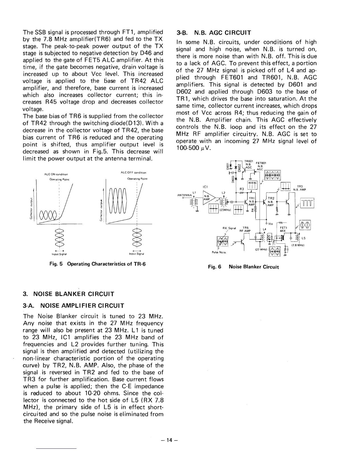
The
SSB
signal
is
processed through FT1, amplified
by the 7.8 MHz amplifier(TR6)
and
fed
to
the
TX
stage.
The peak-to-peak power
output
of
the
TX
stage
is
subjected
to
negative detection .by
046
an?
applied to the gate
of
FET5
ALC
amplifier.
At
this
time,
if
the gate becomes negative, drain voltage
is
increased up
to
about Vcc level. This increased
voltage
is
applied
to
the
case
of
TR42
ALC
amplifier,
and
therefore,
base
current
is
incr~as~d
which
also
increases collector current; this
in-
creases
R45 voltage drop
and
decreases
collector
voltage.
The
base
bias
of
TR6
is
supplied
from
the collector
of
TR42
through the switching
diode(013).
With a
decrease in the collector voltage
of
TR42,
the
base
bias current
of
TR6
js
reduced
and
the operating
point
is
shifted, thus
amplifier
output
level
is
decreased
as
shown in Fig.5. This decrease
will
limit
the power
output
at the antenna terminal.
ALC
ON
con
di
tion
Ope
rating Poi nt
A LC 0 F F cond ition
Operating P
oint
Input
Signal
Input
Signal
Fig. 5 Operating Characteristics
of
TR-6
3. NOISE
BLANKER
CIRCUIT
3-A. NOISE
AMPLIFIER
CIRCUIT
The Noise Blanker
circuit
is
tuned
to
23 MHz.
Any
noise
that
exists in the 27 MHz frequency
range
will
also
be
present at 23 MHz. L 1
is
tuned
to 23 M Hz, I C 1 ampl ifies the 23 M Hz band
of
frequencies and L2 provides
further
tuning. This
signal
is
then amplified
and
detected (utilizing
~he
non-I inear characteristic
portion
of
the operating
curve)
by
TR2, N.B. AMP. Also, the
phase
of
the
signal .
is
reversed in
TR2
and
fed
to
the
base
of
TR3
for
further
amplification.
Base
current flows
when a pulse
is
applied; then the
C-E
impedance
is
reduced
to
about 10-20 ohms. Since the col-
lector
is
connected
to
the
hot
side
of
L5
(RX
7.8
MHz), the primary side
of
L5
is
in
effect
short-
circuited
and
so
the pulse noise
is
eliminated
from
the Receive signal.
J..B.
N.B. AGC
CIRCUIT
In
some
N.B. circuits, under conditions
of
high
signal
and
high noise, when N.B.
is
turned on,
there
is
more noise than
with
N.B.
off.
This
is
due
to
a lack
of
AGC.
To
prevent this effect, a
portion
of
the 27 MHz signal
is
picked
off
of
L4
and
ap-
plied through FET601
and
TR601, N.B. AGC
amplifiers. This signal
is
detected by 0601
and
0602
and applied through
0603
to
the
base
of
TR
1,
which drives the
base
into
saturation.
At
the
same
time, collector current increases, which drops
most
of
Vcc
across
R4; thus reducing the gain
of
the N.B.
Amplifier
chain. This AGC effectively
controls the N.B. loop
and
its
effect
on the 27
MHz
RF
amplifier
circuitry.
N.B.
AGe
is
set
to
operate
with
an
incoming 27 MHz signal level
of
100-500
J1
V.
L1
ANTENNA
t
~
i
lel
;;
<0
o
RX. Signal
/
-/
Pulse
N
oi
..
Fig. 6 Noise Blanker Circuit
-14
-