RK3288 Hardware Design Guide
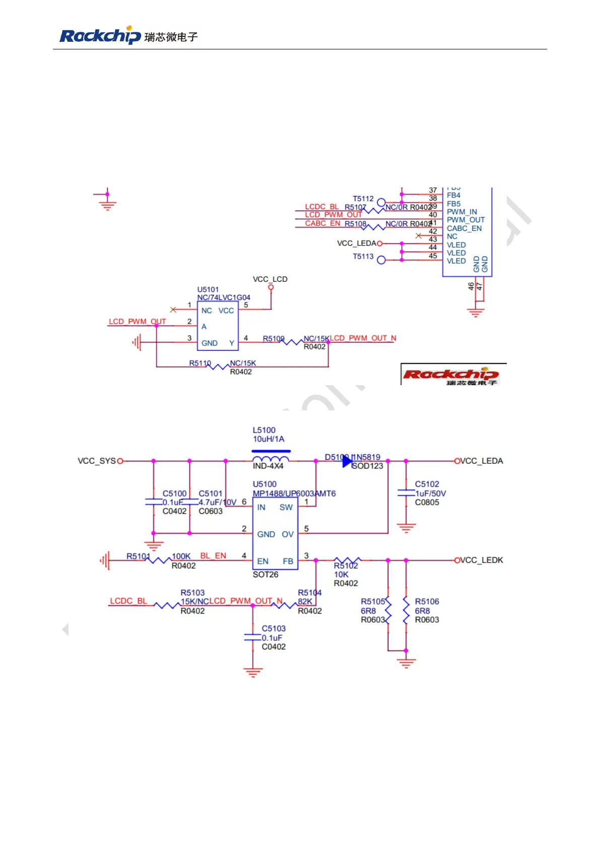
Reserve CABC control circuit in MIPI, LVDS screen drive circuit is shown as in Fig 15-5. If
CABC is not applied, resistor R5107, R5108, R5109, R5110 and inverter U5101 is not
necessary in SMT, backlight voltage regulator circuit in Fig 15-6 can be used instead, which is
controlled by CPU PWM, and if PWM duty ratio is higher, screen brightness is lower; if CABC is
in use, 0R resistor R5107, R5108 should be SMT, inverter U5101 and resistance R5109,R5110
can be decided to SMT or not based on screen specification(duty ratio is higher, screen
brightness is higher or lower).
Fig 15-5
Fig 15-6
For the design of LCM, make sure LCM level can match IO level, as shown in Fig 15-7, dual
MIPI screen VDDIO is 1.8V, the distribution of voltage should be used in LCD_EN, LCD_RST
signals.