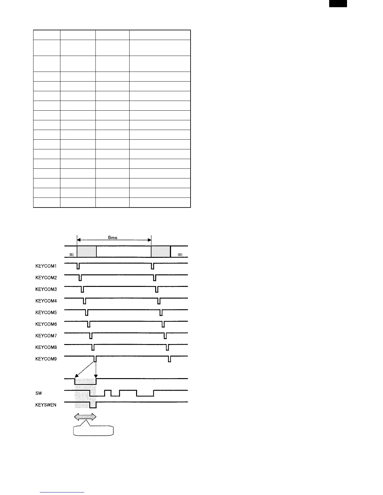
C. LCD panel pin arrangement
Pin No. Signal name Input/Output Remark
1 LCDRS Input
H: Data input;
L: Instruction input
2 LCDRW Input
H: Data read;
L: Data write
3 LCDE Input Enable signal
4 DB0 Input Not used.
5 DB1 Input Not used
6 DB2 Input Not used
7 DB3 Input Not used
8 LCDB4 Input Data bus line
9 LCDB5 Input Data bus line
10 LCDB6 Input Data bus line
11 LCDB7 Input Data bus line
12 V
SS
–0V
13 V
DD
– +5.2V
14 Vin – +5.2V
15 V5 – LCD drive power
16 GND – Frame GND
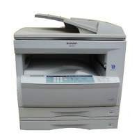
D. Key scan input process diagram
LCD display data
process time (B)
Key scan
process
time (A)
Key scan
process
time (A)
Key SW effective period
input
AR-F152
12 – 22