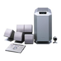
HT-CN150DVW
68
IC801, ESS DVD SERVO (ES6603S)
Pin Description:
Table 1 lists the pin descriptions for the ES6603.
The pound symbol (#) iindicates an active-low signal.
Table 1 ES6603 Pin Descriptions List
Name Pin Numbers I/O Definition
DVDRFP,
DVDRFN
1,2 I Differential RF signal attenuator inputs.
A2,B2,C2,D2 3:6 I
AC coupled photo detector interface inputs for the differential phase detector (DPD) from the main
beam photo matrix.
CP,CN 7,8 - Differential phase tracking low-pass filter pins. Connect CP to CN via capacitors.
D,C,B,A 9:12 I Photo detector interface inputs from the main beam photo matrix.
D_D,CD_C,
CD_B,CD_A
13:16 I CD photo detector interface inputs from the main beam photo matrix
CD_F,CD_E 17, 18 I
CD photo detector interface inputs from the CD side beam photo detector, used for CD tracking
detection.
VPB 19 P Servo block power supply.
VC 20 O Reference voltage out (VPB/2).Output impedance is less than 50Ω.
DVDLD 21 O DVD APC output; controls laser power for DVD.
CDLD 22 O CD APC output; controls laser power for CD.
DVDPD 23 I DVD APC input.
CDPD 24 I CD APC input.
VNB 25 G Serve block ground.
LDON 26 I APC On/Off control. A high level activates LD output. (open is low)
MIRR 27 O Mirror detect output.
MP, MB 28, 29 I Mirror top and bottom hold pins. Connected to VPB pin 19 via capacitors.
MLPF 30 I Mirror low-pass filter pins. Connected to VPB pin 19 via a capacitor.
MIN 31 I RF input signal for mirror. AC coupled inputs for the mirror detection circuit from MEVO pin 32.
MEVO 32 O RFDC bottom envelope out. Pull-In or bottom clamped RF envelope signal ouptut for mirror detection.
LINK 33 I,O
Linking Signal In/Mirror Monitor Out. In the linking area, the mirror and
tracking error outputs are disabled when this pin goes high. When the monitor
output signal is selected by the Control H register, mirror-related signals can be observed.
DFT 34 O
Defect output. When the Pull-in signal level is below the detection level, or when the RF signal level is
below the detection level, the DFT output goes high. The defect output is selected by the serial port.
TPH 35 I Pull-In top hold. Connected to VPB pin 19 via a capacitor.
V125 36 O 1.25V servo block reference voltage output.
V25 37 P 2.5V servo output reference power supply.
PI 38 O
Pull-In signal out. The summing signal output of A, B, C, D or CD_A, CD_B, CD_C, or CD_D. Refer-
ence to V25/3.
TE 39 O Tracking error output reference to V125 pin 36.
FE 40 O Focusing error output reference to V125 pin 36.
CE 41 O Center error output reference to V125 pin 36.
MNTR 42 O Monitor out signal. Output is selectable by register settings.
LCN,LCP 43, 44 I Lens shift offset cancellation low-pass filter pins. Connect LCN to LCP via a capacitor.
V33 45 P 3.3V output buffers power supply.
SCLK 46 I Serial clock from ES66x8.
SDATA 47 I/O Serial data I/O
SDEN 48 I Serial data enable. Enabled by an active-high signal.
RX 49 I Reference resistor. Connected to ground via a 12.0kΩ, 1% resistor.