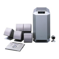
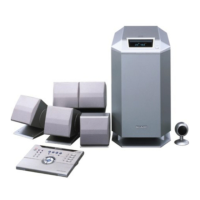
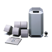
HT-CN150DVW
86
IC203, 4 Banks x IM x 16 Bit Synchronous DRAM (HY57V641620G)
Pin Configuration:
Pin Description:
Pin Pin Name Description
CLK Clock The system clock input. All other inputs are registered to the SDRAM on the rising edge of CLK.
CKE Clock Enable
Controls internal clock signal and when deactivated, the SDRAM will be one of the states
among power down, suspend or self refresh.
CS
Chip Select Enables or disables all inputs except CLK, CKE and DQM
BA0, BA1 Bank Address
Selects bank to be activated during RAS
activity.
Selects bank to be read/written during CAS
activity.
A0 ~ A11 Address
Row Address: RA0 ~ RA11, Column Address: CA0 ~ CA7
Auto-pre-charge flag: A10
RAS
, CAS, WE
Row Address Strobe, Column
Address, Strobe, Write Enable
RAS, CAS and WE define the operation
Refer function truth table for details
LDQM, UDQM Data Input/Output Mask Controls output buffers in read mode and masks input data in write mode
DQ0 ~ DQ15 Data Input/Output Multiplexed data input/output pin
VDD/VSS Power Supply/Ground Power supply for internal circuits and input buffers
VDDQ/VSSQ Data Output Power/Ground Power supply for output buffers
NC No Connection No connection
1
2
3
4
5
6
7
8
9
10
11
12
13
14
15
16
17
18
19
20
21
22
23
24
25
26
27
VDD
DQO
VDDQ
DQ1
DQ2
VSSQ
DQ3
DQ4
VDDQ
DQ5
DQ6
VSSQ
DQ7
VDD
LDQM
/WE
/CAS
/RAS
/CS
BA0
BA1
A10/AP
A0
A1
A2
A3
VDD
VSS
DQ15
VSSQ
DQ14
DQ13
VDDQ
DQ12
DQ11
54pin TSOP II
400ml x 875ml
0.8mm pin pitch
VSSQ
DQ10
DQ9
VDDQ
DQ8
VSS
NC
UDQM
CLK
CKE
NC
A11
A9
A8
A7
A6
A5
A4
VSS
54
53
52
51
50
49
48
47
46
45
44
43
42
41
40
39
38
37
36
35
34
33
32
31
30
29
28