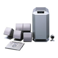
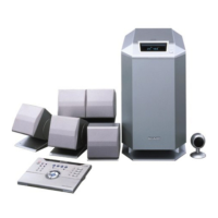
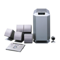
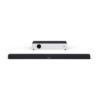
HT-CN150DVW
75
Name Pin Numbers I/O Definition
TESTDA 176 O Test DA output.
FGIN 177 I Spindle hall sensor input.
PHOI 178 I Sledge photo interrupt signal input.
SCSJ 179 O Chip selection signal to RF chip (serial data enable).
SDATA 180 I/O Data signal from/to RF chip.
SCLK 181 O Serial clock source to RF chip.
DFCT 182 I Defect flag input signal.
LDC 183 O Laser diode on/off control output.
SPDON 184 O Spindle power driver on/off control output.
GPIO [9:4] 187:192 I/O General-purpose input/output used for servo control; (5V tolerant input).
EAUX [3:0] 193:196 I/O Extended auxiliary ports; (5V tolerant input).
I
2
CDATA
199
I/O
I
2
C clock I/O; (5V tolerant input).
AUX0 I/O Auxiliary port (open collector); (5V tolerant input).
I
2
C_CLK
200
I/O
I
2
C clock I/O; (5V tolerant input).
AUX1 I/O Auxiliary port (open collector); (5V tolerant input).
LOW#
201
O I/O Write strobe (LCS1) (active-low).
HSYNC# I/O Horizontal sync (active-low); (5V tolerant input).
AUX2 I/O Auxiliary port ; (5V tolerant input).
IOR#
202
O I/O Read strobe (LCS1) (active-low).
VSYNC# I/O Vertical sync (active-low); (5V tolerant input).
AUX3 I/O Auxiliary port ; (5V tolerant input).
C2PO
203
I Error correction flag form CD; (5V tolerant input).
AUX4 I/O Auxiliary port ; (5V tolerant input).
AUX [6:5] 204, 205 I/O Auxiliary port ; (5V tolerant input).
IR
206
I Infrared remote control input; (5V tolerant input).
AUX7 I/O Auxiliary port ; (5V tolerant input).
RESET# 207 I Reset input (active-low); (5V tolerant input).
VD33 1,10,19,35,44,53,62,96,126,185 P I/O power supply.
VID_XI 2 I Crystal input.
VID_XO 3 O Crystal output.
CLK 4 I System clock.
DMA [11:0] 5:8 11:17, 20 O DRAM address bus.
V33 9,18,34,43,52,61,78,95,119,127,186,208 G Ground for I/O power supply.
DCAS# 21 O DRAM column address strobe (ative-low).
DCS[1:0]# 22,23 O DRAM chip select (ative-low).
DRAS[2:0]# 24,25,28 O DRAM row address strobe (ative-low).
VSS 26,70,86,137,197 G Ground for core power supply.
VDD 27,71,87,138,198 P Core power supply.
DSCK_EN
29
O DRAM clock enable output.
DOE# O DRAM output enable (ative-low).
DWE# 30 O DRAM write enable (ative-low).
DB[15:0] 31:33,36:42,45:50 I/O DRAM data bus.
DSCK 51 O Output clock to DRAM.
DQM 54 O Data input/output mask
LA[21:0] 56:60, 63:69. 72:77, 80:82 O RISC port address bus.
LCS[3:0]# 83:85,88 O RISC port chip select (active-low).
LWRLL# 89 O RISC port low-byte write enable (active-low).