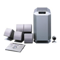
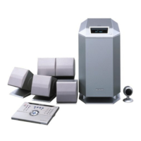
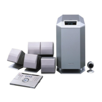
HT-CN150DVW
77
ES6629 DEVICE INTERFACES
Table 2 lists the devices interfaces for the ES6629.
Table 2 ES6629 Device Interfaces
Name Pin Numbers I/O Definition
Audio Port Interface
101 I Audio receive serial data input [RSD]; (5V tolerant input).
102 I Audio receive bit clock input [RBCK]; (5V tolerant input).
103 I Audio receive frame sync input [RWS]; (5V tolerant input).
116 O Audio transmit frame sync output. [TWS].
117, 118, 120, 121 O Audio transmit serial data outputs. [TSD[3:0]].
122 I/O Audio DAC master clock [MCLK].
123 O Audio transmit bit clock output [TBCK].
124 O Sony/Philips Digital Interface audio output.
125 I Sony/Philips Digital Interface audio input [SPDIF_IN]
Auxiliary Port Interface
193:196 I/O Extended auxilliary ports [EAUX[3:0]] ; (5V tolerant input).
199:200 I/O Open collector auxilliary ports [AUX[1:0]]; (5V tolerant input).
201:206 I/O Primary auxilliary port I/Os [AUX[7:2]]; (5V tolerant input).
Clock Interface and
reset
2 I 27-MHz crystal clock input [VID_XI].
3 0 27-MHz crystal clock output [VID_XO].
4 I System clock. [CLK].
29 O DRAM clock enable output [DSCK_EN].
51 O Output clock [DSCK] to video memory (DRAM).
116:118 I Clock frequency select PLL outputs [SEL_PLL[2:0]].
207 I Reset input (active-low) [RESET#]; (5V tolerant input).
Display Interface
106:110, 113:115 O Pixel data outputs [YUV[7:0]].
201 I/O Horizontol sync [HSYNC#]; (5V tolerant input).
202 I/O Vertical sync [VSYVC#]; (5V tolerant input).
EPROM/Flash ROM
and RISC Port Interface
55:60, 63:69, 72:77, 80:82 O RISC port address bus [LA[21:0]] to EPROM or Flash memory.
83:85 O RISC port chip select outputs [LCS[2:0]#] to EPROM or Flash memory.
89 O
RISC port low-byte write enable output [LWRLL#] to EPROM or Flash
memory.
90 O RISC port output enable [LOE#] to EPROM and Flash memory.
91:94, 97:100 I/O
RISC port data bus [LD[7:0]] to EPROM or Flash memory; (5V tolerant
input).
Filter and Reference
Voltage Interface
106 I Video DAC reference voltage input [VREF].
107 I Compensation input [COMP].
Front Panel
Display Interface
206 I Infrared remote control input [IR]; (5V tolerant input).
General-Purpose 187:192 I/O General-purpose I/O [GPIO(9:4)]; (5V tolerant input).
I
2
C Bus Interface
199 I/O
I
2
C data I/O [12C_DATA]; (5V tolerant input).
200 I/O
I
2
C clock I/O [12C_CLK]; (5V tolerant input).
Power and Ground 1,10,19,35,44,53,62,79,96,126,185 P I/O power supply [VD33].
9,18,34,43,52,61,78,95,119,127,186,
208
G I/O ground [VS33].
26,70,86,137,197 G Ground for core power [VSS].
27,71,87,138,198 P Core power supply [VDD].
104 P Power supply for PLL block. [VD33_PL].
105 G Ground for PLL Bblock [VD33_PL].
111 P Power supply for video DAC [VD33_DA].
112 G Ground for video DAC [VS33_DA].