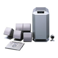
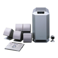
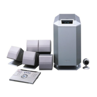
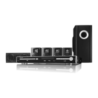
HT-CN150DVW
79
Name Pin Numbers I/O Definition
Servo Control and Data
Interface
133:136 O To monitor servo status [FLAG(3:0)].
177 I Spindle hall Sensor input [FGIN].
178 I Sledge photo interrupt signal input [PHOI].
179 O Chip selection signal to RF chip (serial data enable) [SCSJ].
180 I/O Data signal from/to RF chip [SDATA].
181 O Serial clock source to RF chip [SCLK].
182 I Defect flag input signal [DFCT].
183 O Laser diode on/off control output [LDC].
184 O Spindle power driver on/off control output [SPDON].
187:192 I/O
General-purpose input/output used for servo control [GPIO(9:4)]; (5V
tolerant input.)
Servo DVD-RAM
Interface
128 O DVD-RAM wobble detector circuit clock source to preamp [WBLCLK].
129 O DVD-RAM wobble output [WBL].
130 O DVD-RAM land/groove flag [LG].
131 I DVD-RAM header position index 2 [IP2}.
132 I DVD-RAM header position index 1 [IP1].
System Memory
Interface
5:8, 11:17, 20 O DRAM address bus [DMA(11:0)].
21 O Memory column address strobe output [DCAS#].
22,23 O DRAM chip select outputs [DCS(1:0)#].
24,25,28 O Memory row address strobe output [DRAS(2:0)#].
29 O Memory output enable [DOE#].
30 O Memory write enable output [DWE#].
31:33, 36:42, 45:50 I/O Memory data bus [DB(15:0)].
51 O Output clock to DRAM [DSCK].
54 O Memory data I/O mask output [DQM].
Video DAC Interface
109 O CVBS/chroma signal [FDAC] for simultaneous mode.
110 O Composite component signal [VDAC] for YUV mode.
113 O Luma component signal [YDAC] for YUV mode and Y/C processing.
114 O Chrominance component signal [CDAC] for Y/C processing.
115 O Chrominance component signal [UDAC] for YUV mode.