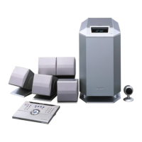
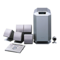
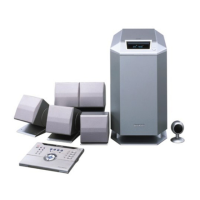
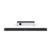
HT-CN150DVW
99
IC201A, 8-BIT OTP microcontroller (HT48R05A-1)
Pin Description:
Pin No Pin Name I/O
ROM Code
Option
Description
4~1,
18~15
PA0~PA7 I/O
Pull-high*
Wake-up
Bidirectional 8-bit input/output port. Each bit can be configured as wake-up input by ROM
code option.Software instructions determine the CMOS output or schmitt trigger input with
a pull-high resistor (determined by pull-high options)
7
6
5
PB0/BZ
PB1/BZ
PB2
I/O
Pull-high*
I/O or
BZ/BZ
Bidirectional 3-bit input/output port. Software instructions determine the CMOS output or
schmitt trigger input with a pull-high resistor (determined by pull-high options).
The PB0 and PB1 are pin-shared with the BZ and BZ,
respectively. Once the PB0 and
PB1 are selected as buzzer driving outputs, the output signals come from an internal PFD
generator (shared with timer/event counter)
8 VSS - - Negative power supply, ground.
9
10
PC0/INT
PC1/TMR
I/O Pull-high*
Bidirectional I/O lines. Software instructions (determine the CMOS output or SCHMITT
trigger input with a pull-high options). The external interrupt and timer input are pin-shared
with the PC0 and PC1, respectively. The external interrupt input is activated on a high to
low transition.
11 RES
I - Schmitt trigger reset input. Active low
12 VDD - - Positive power supply
13
14
OSC1
OSC1
I
O
Crystal or RC
OSC1, OSC2 are connected to an RC network or Crystal(determined by ROM code
option) for the internal system clock. In the case of RC operation, OSC2 is the output ter-
minal for 1/4 system clock.