– 39 –
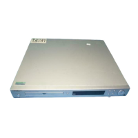
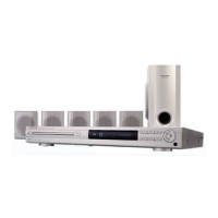
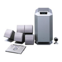
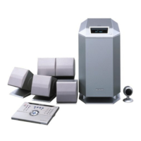
HT-CN400DVH/HT-CN400DVE/HT-CN500DVH/HT-CN500DVE
FUNCTION TABLE OF IC
IC801 92LRCI6560-001: Motor Driver (LA6560)
1 FWD Output change pin (FWD) for 5CH (VLO), logic input for loading block.
2 REV Output change pin (REV) for 5CH (VLO), logic input for loading block.
3 VCC2 Power supply for CH3, 4 and 5.
4 VLO- Loading output (-).
5 VLO+ Loading output (+).
6 VO4+ Output pin (+) for channel 4.
7 VO4- Output pin (-) for channel 4.
8 VO3+ Output pin (+) for channel 3.
9 VO3- Output pin (-) for channel 3.
10 VO2+ Output pin (+) for channel 2.
11 VO2- Output pin (-) for channel 2.
12 VO1+ Output pin (+) for channel 1.
13 VO1- Output pin (-) for channel 1.
14 VCC1 Power supply for CH1, 2 (BTL).
15 VIN1 Input pin for channel 1.
16 VIN1-A OP-AMP input AMP-A input pin (-).
17 VIN1+A OP-AMP input AMP-A input pin (+).
18 VIN1-B Input AMP-B input pin (-) for channel 1.
19 VIN1+B Input AMP-B input pin (+)for channel 1.
20 VIN2 Input pin for channel 2, input AMP output.
21 VIN2- Input pin (-) for channel 2.
22 VIN2+ Input pin (+) for channel 2.
23 VIN3 Input pin for channel 3, input AMP output.
24 VIN3- Input pin (-) for channel 3.
25 VIN3+ Input pin (+) for channel 3.
26* REG-IN PNP transistor base connected.
27* REG-OUT 5 V power output to which the PNP transistor collector connected.
28* VREF-OUT CH1 reference voltage output. Outputs internal VREF (2.5 V:TYP) or external VREF.
29 VIN1 Pin for changeover between input AMP-A/internal VREF (TYP2.5 V) and input AMP-B/external VREF.
(VREF)-SW
30 VREF-IN Reference voltage applied pin.
31 VIN4+ Input pin (+) for channel 4.
32 VIN4- Input pin (-) for channel 4.
33 VIN4 Input pin for channel 4, input AMP output.
34 MUTE All BTL AMP output ON/OFF.
35 VCONT Loading output voltage setting.
36 S-GND Signal system GND.
Port NamePin No.
Function
In this unit, the terminal with asterisk mark (*) is (open) terminal which is not connected to the outside.
* Center frame (FR) becomes GND for the power system (P-GND). Set this to the minimum potential together with S-GND.