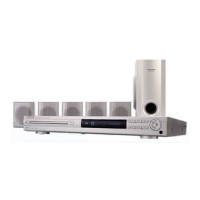
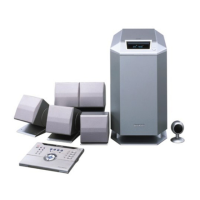
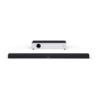
HT-CN410DVH
55
IC303, 192 kHz Multi-bit audio A/D Converter (CS5342)
Figure 8: FUNCTIONAL BLOCK DIAGRAM
IC303, 192 kHz Multi-bit audio A/D Converter (CS5342)
Pin Description:
Table 1 ES6602 Pin Description List (Continued)
Names Pin Numbers I/O Definitions
VNA 51 G RF block and serial port ground.
FNN, FNP 52, 53 O Differential outputs of equalizer/filter.
DIP, DIN 54, 55 I
Differential analog input to the RF single-end output buffer and full
wave rectifier.
BYP 56 I AGC amplifier gain bypass. Tied to VPA via a capacitor.
RFAC 57 O Single-ended RF output.
VPA 58 P RF block and serial port power supply.
AIP, AIN 59, 60 I Differential AGC amplifier inputs.
ATON ATOP 61, 62 O Differential attenuator outputs.
RFSIN 63 I Single-ended RF signal attenuator input.
VQ
REFGND
GND
AINR
AINL
FILT+
SCLK
LRCK SDOUT MCLK
V
L
2.5V - 5.0V
VD
3.3V - 5.0V
VA
3.3V - 5.0V
RST
M0
M1
Serial Output Interface
Voltage Reference
LP Filter
LP Filter
DAC
Q
Q
DAC
S/H
S/H
+
-
+
-
Digital
Decimation
Filter
High
Pass
Filter
High
Pass
Filter
Digital
Decimation
Filter
M0
MCLK
VL
SDOUT
GND
VD
SCLK
LRCK
M1
FILT+
REFGND
VA
AINR
VQ
AINL
RST
116
15
14
13
12
11
10
9
2
3
4
5
6
7
8