LC-26SA1E/RU, LC-32SA1E/RU
7 – 13
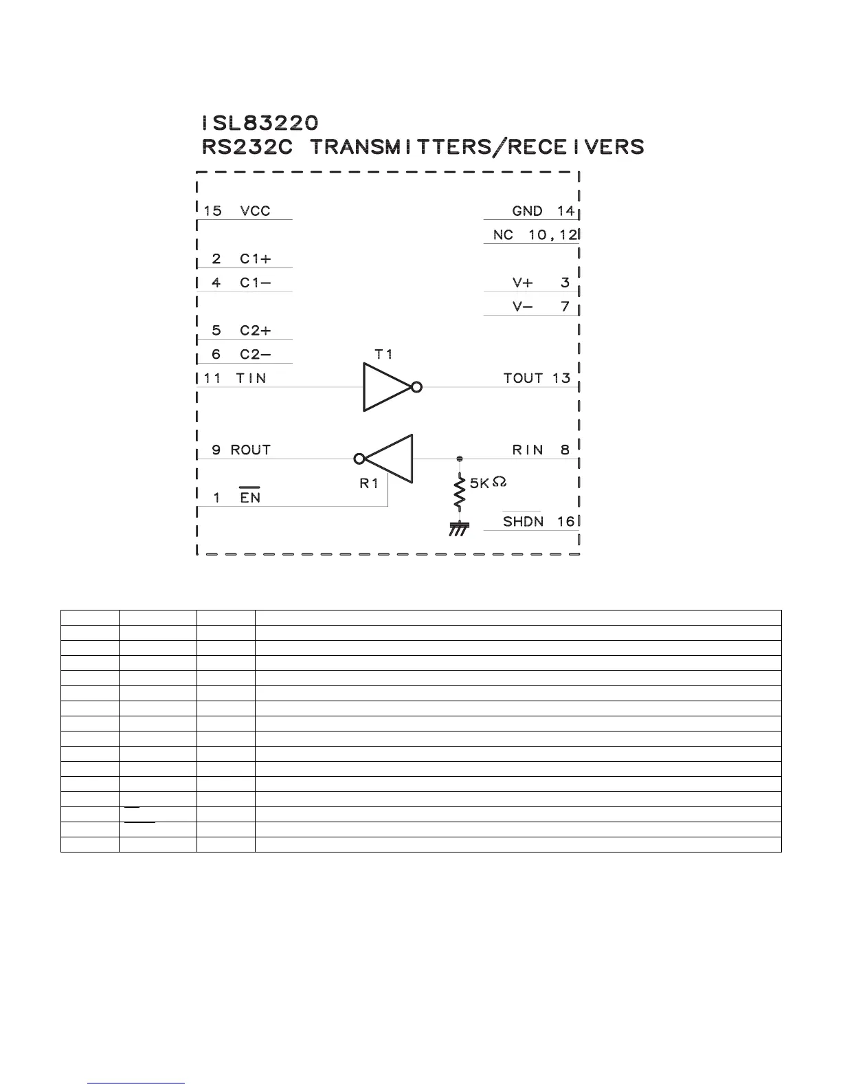
2.5. IC2301 (VHIISL83220-1Y)
2.5.1 Block Diagram
2.5.2 Pin Connections and short description
Pin No. Pin Name I/O Pin Function
15 VCC – System power supply input (3.0V to 5.5V).
3 V+ – Intemally generated positive transmitter supply (+5.5V).
7 V- – Internally generated negative transmitter supply (-5.5V).
14 GND – Ground connection.
2 C1+ – External capacitor (voltage doubler) is connected to this lead.
4 C1- – External capacitor (voltage doubler) is connected to this lead.
5 C2+ – External capacitor (voltage doubler) is connected to this lead.
6 C2- – External capacitor (voltage doubler) is connected to this lead.
11 TIN I TTL/CMOS compatible transmitter inputs.
13 TOUT O ±15KV ESD Protected, RS-232 level (nominally ±5.5V) transmitter output.
8RIN I±15KV ESD Protected, RS-232 compatible receiver inputs.
9 ROUT O TTL/CMOS level receiver output.
1EN
O Active low receiver enable control; doesn't disable ROUTB output.
16 SHDN
– Active low input shuts down transmitters and on-board power supply, to place device in low power mode.
10 N.C. – No internal connection.