LC-26SA1E/RU, LC-32SA1E/RU
7 – 14
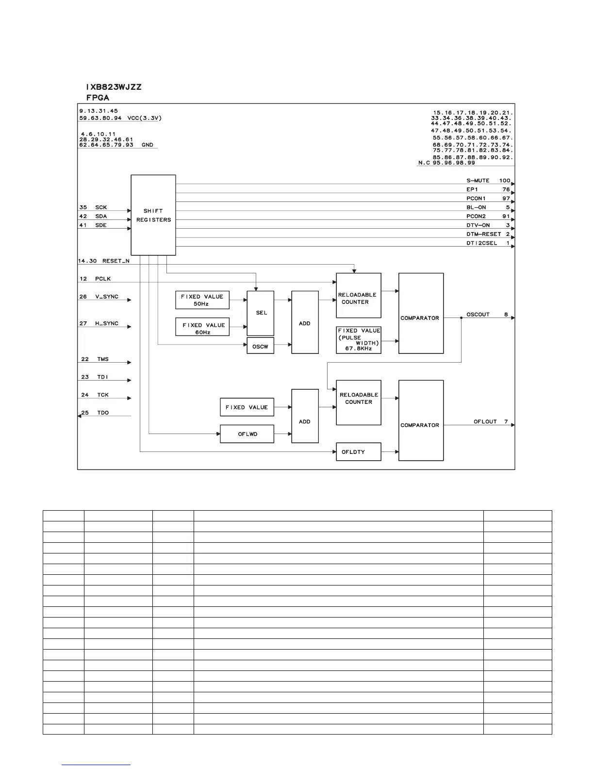
2.6. IC1710 (RH-IXB823WJZZQ)
2.6.1 Block Diagram
2.6.2 Pin Connections and short description
Pin No. Pin Name I/O Pin Function Sheet Name
1 EXP [7] O Outport [7] DTI2CSEL
2 EXP [6] O Outport [6] DTM_RESET
3 EXP [5] O Outport [5] DTV_ON
4 GND* – Ground N.C.
5 EXP [3] O Outport [3] BL_ON
6 GND* – Ground N.C.
7 OFLOUT O OFL signal output OFLOUT
8 OSCOUT O OSC signal output OSCOUT
9 VCCIO1 – VCC (3.3V) FPGA_VCC
10 GNDIO – Ground Ground.
11 GNDINT – ground. Ground.
12 PCLK I Reference clock input PCLK
13 VCCINT – VCC (3.3V) FPGA_VCC
14 GCLR I RESET terminal. L: RESET, H: Normal RESET_N
15 GND* – N.C. N.C.
16 GND* – N.C. N.C.
17 GND* – N.C. N.C.
18 GND* – N.C. N.C.
19 GND* – N.C. N.C.
20 GND* – N.C. N.C.