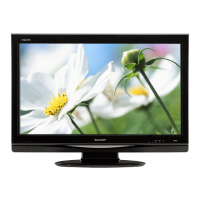
LC-32X20E/S/RU, LC-37X20E/S/RU
5 – 5
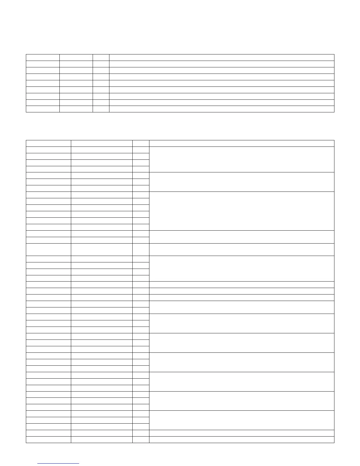
2. Detailed ICs Information
2.1. IC402 (VHiBD9305AF-1Y)
2.1.1 Pin Connections and short description
2.2. IC506 (VHiMM3151XQ-1Q)
2.2.1 Pin Connections and short description
Pin No. Pin Name I/O Pin Function
1 RT — Timing resistor external terminal
2 CT — Timing capacitor external terminal
3 ENB I Control input terminal
4 GD O Gate drive output terminal
5 VCC — Power terminal
6 GND — Ground terminal
7 COMP O Error amplifier output terminal
8 FB I Error amplifier inversion input terminal
Pin No. Pin Name I/O Pin Function
69 C1 I Chroma signal input
75 C2 I
1C3 I
7C4 I
70 S1 I The terminal which detects the connection state of S-connector.
76 S2 I
2S3 I
65 V1 I Composite signal input.
71 V2 I
77 V3 I
3V4 I
9V5 I
15 V6 I
68 S2-1 I The terminal which detects the aspect ratio information of S-connector.
74 S2-2 I
80 S2-3/ FS3 I The terminal which detects the aspect ratio information of S-connector, or which detects
the voltage of FS pin of a scart connector.
67 Y1 I Luminance signal input.
73 Y2 I
79 Y3 I
5Y4 I
14 ADR I Slave address select pin.
16 BIAS I BIAS
32 L13 I The terminal which detects the number of scanning lines information on D-connector.
20 L11/ FS1 I The terminal which detects the number of scanning lines information on D-connector, or
which detects the voltage of FS pin of a scart connector.
26 L12/ FS2 I
21 CY1 I Component Y-signal input.
27 CY2 I
33 CY3 I
22 L21 I The terminal which detects the I/P information of D-connector.
28 L22 I
34 L23 I
24 L31 I The terminal which detects the aspect ratio information of D-connector.
30 L32 I
36 L33 I
23 PB1 I Colour difference PB-signal input.
29 PB2 I
35 PB3 I
25 PR1 I Colour difference PR-signal input.
31 PR2 I
37 PR3 I
38 SW1 I The terminal which detects the connection state of D-connector.
40 SW2 I
42 SW3 I
45 SDA I/O Data I/O of I2C bus
46 SCL I Clock input of I2C bus
 Loading...