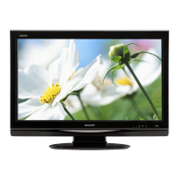
LC-32X20E/S/RU, LC-37X20E/S/RU
5 – 9
2.6. IC1404 (VHiAK4683EQ-1Q)
2.6.1 Block Diagram
22 SCLKOUT1 O Bit clock #1 out. Used to receive input serial data.
23 SCLKOUT2 O Bit clock #2 out. Used to clock output serial data.
15 SDA1 I/O I2C port #1 data (always a slave)
17 SDA2 I/O I2C port #2 data (always a slave)
11 SDIN1 I Pull-down Serial data input 1
12 SDIN2 I Pull-down Serial data input 2
13 SDIN3 I Pull-down Serial data input 3
14 SDIN4 I Pull-down Serial data input 4
27 SDOUT1 O Serial data output 1
26 SDOUT2 O Serial data output 2
25 SDOUT3 O Serial data output 3
24 SDOUT4 O Serial data output 4
2 VR_PLL — Internal regulator. This pin must not be used to power external devices.
3 XTALI I Oscillator input (connect to ground when not in use)
4 XTALO O Oscillator output
28 VR_DIG --- Internal regulator. This pin must not be used to power external devices.
Pin No. Pin Name I/O Pin Function
 Loading...