76
LC-32LE63x
LC-40LE63x
LC-46LE63x
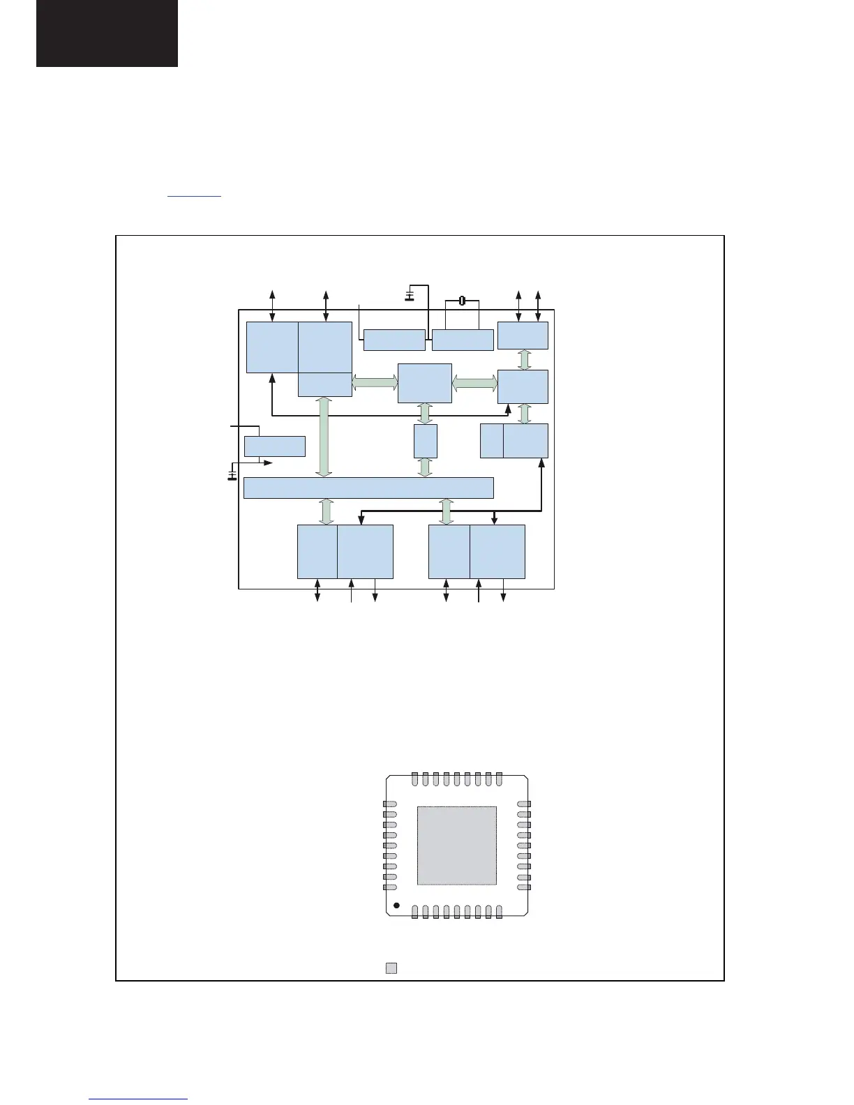
This chapter shows the internal block diagrams and pin
configurations of ICs that are drawn as “black boxes” in the
electrical diagrams (with the exception of “memory” and “logic”
ICs).
8.1 Diagram USB Hub B01C, USB2513B (IC 7F25)
Figure 8-1 Internal block diagram and pin configuration
18770_301_100217.eps
100217
Block diagram
Pinning information
Note : The LED port indicators only apply to USB2513i.
To Upstream
V
BUS
3.3 V
Upstream
PHY
Upstream
USB Data
Repeater
Controller
Serial
Interface
Engine
Serial
Interface
To EEPROM or
SMBus Master
SCL
SDA
Port
Controller
Bus-
Power
Detect/
V
bus
Pulse
PHY#1
USB Data
Downstream
OC
Sense
Switch/
LED
Drivers
USB Data
Downstream
Port
Power
3.3 V
PLL
24 MHz
Crystal
Routing & Port Re-Ordering Logic
Regulator
CRFILT
Port
Power
Regulator
PHY#x
Port #x
OC Sense
Switch Driver/
LED Drivers
TT
#x
TT
#1
...
Port #1
OC Sense
Switch Driver/
LED Drivers
OC
Sense
Switch/
LED
Drivers
...
The ‘x’ indicates the number of available downstream ports: 2, 3, 4, or 7.
Ground Pad
(must be connected to VSS)
SMSC
USB2512/12A/12B
USB2512i/12Ai/12Bi
(Top View QFN-36)
26
VDD33
25
RESET_N
24
HS_IND / CFG_SEL[1]
23
SCL / SMBCLK / CFG_SEL[0]
22
SDA / SMBDATA / NON_REM[1]
21
NC
20
NC
19
VBUS_DET
27
NC
18
NC
17
OCS_N[2]
16
PRTPWR[2] / BC_EN[2]*
15
OCS_N[1]
14
VDD33
13
CRFILT
12
PRTPWR[1] / BC_EN[1]*
11
TEST
10
VDD33
SUSP_IND / LOCAL_PWR / NON_REM[0]
28
VDD33
29
USBDP_UP
31
XTALOUT
32
XTALIN / CLKIN
33
RBIAS
36
VDD33
35
PLLFILT
34
USBDM_UP
30
VDD33
1
USBDM_DN[1]
2
USBDP_DN[1]
3
USBDM_DN[2]
4
USBDP_DN[2]
5
NC
6
NC
7
NC
8
NC
9
Indicates pins on the bottom of the device.