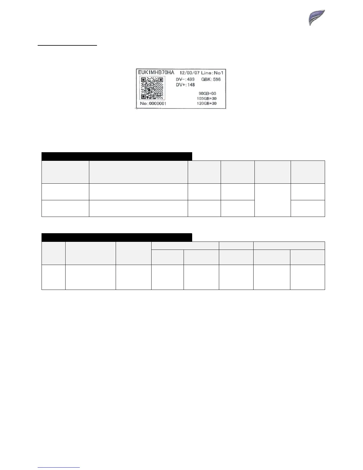
High Voltage Settings
Note: The adjustment value is specified on the information label attached to the High Voltage PWB.
Using Simulation 8-01 (DV Bias Setting) & Sim 8-02 (MC Grid Bias Setting), enter the values
specified, especially after replacing the PCU PWB, EEPROM or following U2 trouble.
DEVELOPING BIAS VOLTAGE – SIMULATION 08-01
Item Content
Setting
Range
Default
Monitor
Connector
& PIN
Actual
Output
Voltage
DVB_K Developing Bias Adjustment value 0-750 496
CN2 Pin
11
5V
DVB_K_PLUS Reverse Developing Bias Voltage 0-250 164
-150 +/-
5V
MAIN CHARGE GRID VOLTAGE – SIMULATION 08-02
Item Content
Setting
Range
Default Monitor Actual Output Voltage
MXM904
MXM1054
MXM1204
Connector
& PIN
MXM904
MXM1054
MXM1204
GB_K
Main Charge
Grid Voltage
Adjustment
200 - 1000 575 605 CN2 Pin 7 -595 +/- 5V
-625 +/-
5V