109
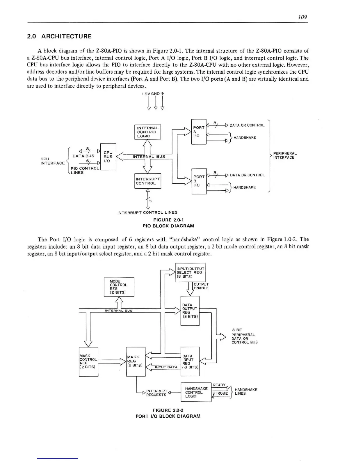
2.0 ARCHITECTURE
A block diagram
of
the Z-80A-PIO
is
shown in Figure 2.0-1 . The internal structure
of
the Z-80A-PIO consists
of
a Z-80A-CPU bus interface, internal control logic, Port A 1/0 logic, Port B
I/0
logic, and interrupt control logic. The
CPU
bus interface logic allows the PIO to interface directly
to
the Z-80A-CPU with no other external logic. However,
address decoders and/or line buffers may be required for large systems. The internal control logic synchronizes the
CPU
data bus to the peripheral device interfaces (Port A and Port B). The two
I/0
ports (A and
B)
are virtually identical and
are
used
to
interface directly to peripheral devices.
{
DATA
:US
CPU
INTERFACE
--=
6
'-f--Dt
PIO
CONTROL
LINES
3
INTERRUPT
CONTROL
LINES
FIGURE
2.0-1
PIO BLOCK
DIAGRAM
Kf--'
8
'-f--1> DATA
OR
CONTROL
1----1>}
HANDSHAKE
PERIPHERAL
INTERFACE
The Port
I/0
logic
is
composed
of
6 registers with "handshake" control logic
as
shown in Figure 1.0-2. The
registers include : an 8 bit data input register, an 8 bit data
output
register, a 2 bit mode control register, an 8 bit mask
register, an 8 bit
input/output
select register, and a 2 bit mask control register.
MASK
MODE
CONTROL
REG
(2
BITS)
CONTROL
1----.........._
REG
(2
BITS)
INPUT/OUTPUT
SELECT
REG
(8
BITS)
DATA
OUTPUT
ENABLE
OUTPUT
1----,
MASK
REG
(8
BITS)
REG
(8
BITS)
'..,------1
PNAPTUAT
REG
_../L...,.,
"'N
P""U-:=T'"'D:-:A-:=T-:-A
-1 ( 8
BITs)
FIGURE
2.0-2
HANDSHAKE
CONTROL
LOGIC
PORT
1/0
BLOCK
DIAGRAM
8 BIT
PERIPHERAL
DATA
OR
CONTROL BUS
READY
___
} HANDSHAKE
STROBE
LINES