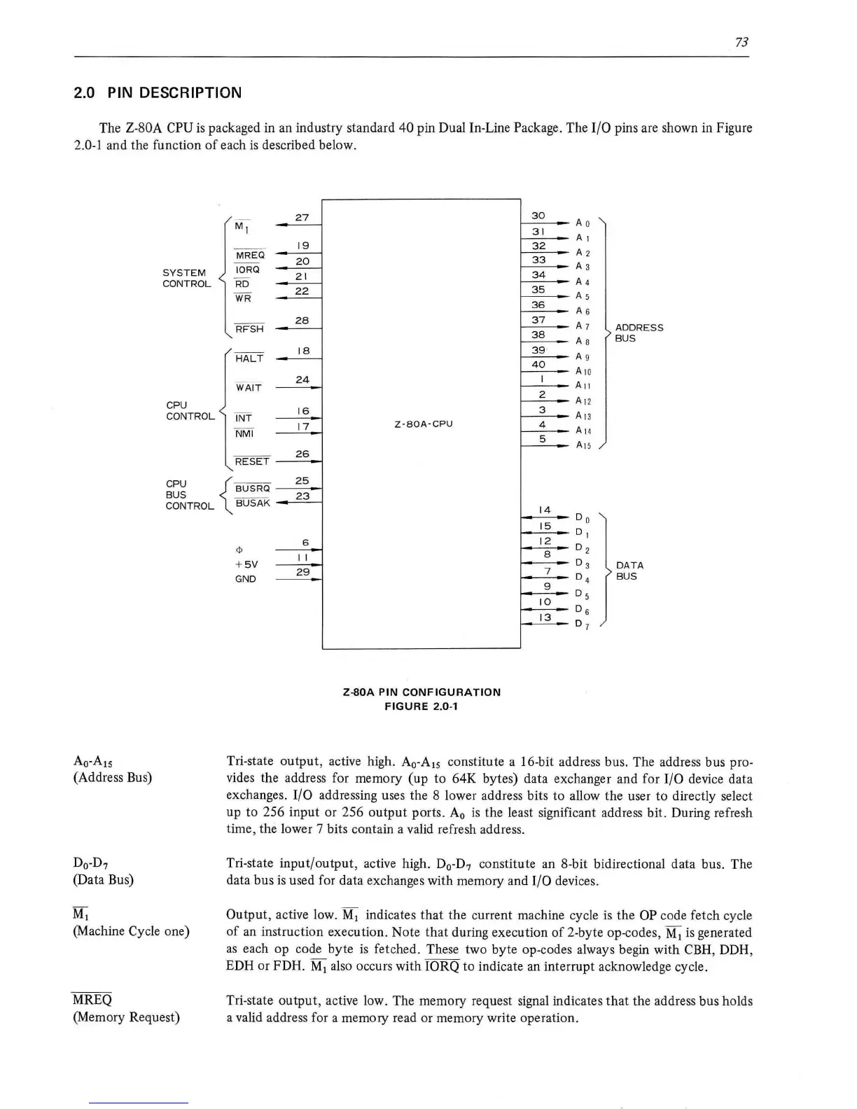
73
2.0 PIN DESCRIPTION
The Z-80A CPU
is
packaged in an industry standard
40
pin Dual In-Line Package. The 1/0 pins are shown in Figure
2.0-1 and the function
of
each
is
described below.
Ao-Ais
(Address Bus)
D
0
-D
7
(Data Bus)
MI
SYSTEM
CONTROL
CPU
MREQ
IORQ
RD
WR
HALT
WAIT
27
19
20
21
22
28
18
24
30
A o
31
AI
32
33
A2
As
34
A4
35
As
36
A6
37
38
A7
ADDRESS
As
BUS
39
·
Ag
40
A 10
I
A11
2
A 12
CONTROL
INT
16
3
Z-SOA·CPU
4
A 13
NMI
RESET
CPU
{BUSRQ
BUS
--
CONTROL
BUSAK
<ll
+ 5V
GND
17
26
25
23
6
II
29
Z-80A
PIN
CONFIGURATION
FIGURE
2.0-1
5
14
15
12
8
7
9
10
13
A1
4
A1
5
Do
Dl
D2
D3
DATA
D4
BUS
Ds
D6
D7
Tri-state output, active high. A
0
-A
15
constitute a 16-bit address bus. The address bus pro-
vides the address for memory
(up
to
64K bytes) data exchanger and for
l/0
device data
exchanges.
1/0 addressing uses the 8 lower address bits to allow the user
to
directly select
up
to
256 input or 256
output
ports. A
0
is
the least significant address bit. During refresh
time, the lower 7 bits contain a valid refresh address.
Tri-state input/output, active high.
D
0
-D
7
constitute an 8-bit bidirectional data bus. The
data bus
is
used for data exchanges with memory and
I/0
devices.
(Machine
Cycle one)
Output,
active low. M
1
indicates
that
the current machine cycle
is
the
OP
code fetch cycle
of
an instruction execution. Note
that
during execution
of
2-byte op-codes, M
1
is
generated
as
each op code byte
is
fetched. These two byte op-codes always begin with CBH, DDH,
EDH or FDH. M
1
also occurs with IORQ to indicate an interrupt acknowledge cycle.
MREQ
(Memory Request)
Tri-state output, active low. The memory request signal indicates
that
the address bus holds
a valid address for a memory read or memory write operation.