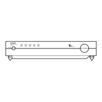
SM-SX1/SX1W
– 46 –
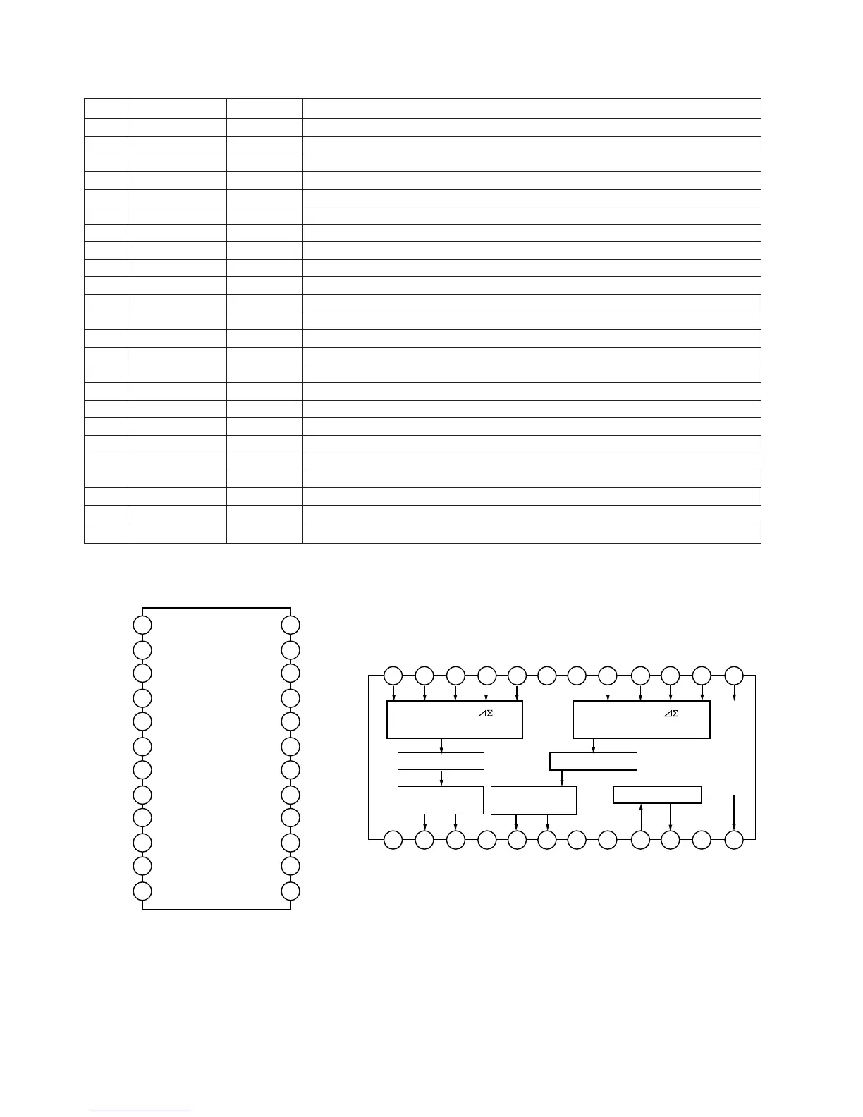
ICA1 RH-iX2815AFZZ: 7th Order Modulation Conversion LSI (IX2815AF)
1 VDDR — R channel digital output section power terminal
2 OUTL (+) Output R channel forward output terminal
3 OUTL (–) Output R channel reverse output terminal
4 GNDD — Digital output section ground terminal
5 OUTR (–) Output L channel reverse output terminal
6 OUTR (+) Output L channel forward output terminal
7 VDDL — L channel digital output section power terminal
8 VDDX — Oscillation section power terminal
9 XI Input Quartz oscillator connection terminal. Clock necessary for the system is generated.
10 XO Output Quartz oscillator connection terminal. Clock necessary for the system is generated.
11 GNDX — Oscillation section ground terminal
12* MCK Output System clock output terminal
13 TEST Input Test terminal. As usual, it is used at "L".
14 NFL1 (+) Input L channel forward signal feedback input terminal
15 NFL2 (–) Input L channel reverse signal feedback input terminal
16 GNDA — Analog ground terminal for AD converter
17 L-CH IN Input L channel analog input terminal
18 L-CH Vref — Reference voltage terminal for L channel
19 R-CH Vref — Reference voltage terminal for R channel
20 R-CH IN Input R channel analog input terminal
21 RESET Input Reset terminal. It is reset with "L".
22 NFR2 (–) Input R channel reverse signal feedback input terminal
23 NFR1 (+) Input R channel forward signal feedback input terminal
24 VDA — Analog current terminal for AD converter
Pin No.
Port Name Input/Output
Function
In this unit, the terminal with asterisk mark (*) is (open) terminal which is not connected to the outside.
1
2
3
4
5
6
7
8
9
10
11
12
24
23
22
21
20
19
18
17
16
15
14
13
VDDR VDDA
NFR1(+)
NFR2(–)
RESET
Rch IN
Rch Vref
Lch Vref
Lch IN
GNDA
NFL2(–)
NFL1(+)
TEST
OUTR(+)
OUTR(–)
GNDD
OUTL(–)
OUTL(+)
VDDL
VDDX
XI
XO
GNDX
MCK
1 2 3 4 5 6 7 8 9 10 11 12
24 23 22 21 20 19 18 17 16 15 14 13
VDA
NFR1(+)
NFR2(–)
RESET
Rch IN
Rch Vre