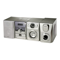
XL-DV60
8 – 3
In this unit, the terminal with asterisk mark (*) is (open) terminal which is not connected to the outside.
IC701 RH-iXA009SJZZ: System Microcomputer (IXA009SJ)
39,40,
41*,42,43,
44,45
S9/T9 to S15/
T15
O • Large current output for VFD display controller segment/digit
47,48,49,
50,52,53,
54,55
S16 to S23 I/O • Output for VFD display controller segment/digit
• Other functions:
High voltage input port: PC0 to PC7
56,57,58,
59,60,61,
62,63
S24 to S31 I/O • Output for VFD display controller segment
• Other functions:
High voltage input port: PD0 to PD7
64,65,66,
67,68,69,
70,71
S32 to S39 I/O • Output for VFD display controller segment
• Other functions:
High voltage input port: PE0 to PE7
73,74,75,
76,77,78,
79,80
S40 to S47 I/O • Output for VFD display controller segment
• Other functions:
High voltage input/output port: PF0 to PF7
81*,82*,
83,84*
S48 to S51 I/O • Output for VFD display controller segment
• Other functions:
High voltage input/output port: PG0 to PG7
11 RES I Reset terminal
12 XT1 I • Input for 32.768kHz crystal oscillation
• Other functions:
General purpose input port
When not in use, connect to VDD1.
AD input port: AN10
13 XT2 I/O • Output for 32.768kHz crystal oscillation
• Other functions:
General purpose input/output port
When not in use, set to oscillation mode and leave open circuit.
AD input port: AN11
15 CF1 I Input terminal for ceramic oscillator
16 CF2 O Output terminal for ceramic oscillator
Pin No. Port Name Input/Output Function
Note1:) The LC876700 series can be mounted onto the circuit board of the LC 876500, LC876600 series.
In this case, the fluorescent character display tube power voltage (minus voltage) is supplied to the FIX0 pin. This would not cause any
error.
S19/PC3
S18/PC2
S17/PC1
S16/PC0
VDD3
S15/T15
S14/T14
S13/T13
S12/T12
S11/T11
S10/T10
S9/T9
S8/T8
S7/T7
S6/T6
S5/T5
S4/T4
S3/T3
S2/T2
S1/T1
S48/PG0
S49/PG1
S50/PG2
S51/PG3
P00
P01
P02
P03
VSS2
VDD2
P04
P05
P06
P07
P10/SO0
P11/SI0/SB0
P12/SCK0
P13/SO1
P14/SI1/SB1
P15/SCK1
S47/PF7
S46/PF6
S45/PF5
S44/PF4
S43/PF3
S42/PF2
S41/PF1
S40/PF0
VDD4
S39/PE7
S38/PE6
S37/PE5
S36/PE4
S35/PE3
S34/PE2
S33/PE1
S32/PE0
S31/PD7
S30/PD6
S29/PD5
S28/PD4
S27/PD3
S26/PD2
S25/PD1
S24/PD0
S23/PC7
S22/PC6
S21/PC5
S20/PC4
FIX0
P16/T1PWML
P17/T1PWMH/BUZ
P30/INT4/T1IN
P31/INT4/T1IN
P32/INT4/T1IN
P33/INT4/T1IN
P34/INT5/T1IN
P35/INT5/T1IN
P36/INT5/T1IN
P37/INT5/T1IN
RES
XT1/AN10
XT2/AN11
VSS1
CF1
CF2
VDD1
P80/AN0
P81/AN1
P82/AN2
P83/AN3
P84/AN4
P85/AN5
P86/AN6
P87/AN7/MICIN
P70/INT0/T0LCP/AN8
P71/INT1/T0HCP/AN9
P72/INT2/T0IN/AN12
P73/INT3/AN13
S0/T0
81
82
83
84
85
86
87
88
89
90
91
92
93
94
95
96
97
98
99
100
50
49
48
47
46
45
44
43
42
41
40
39
38
37
36
35
34
33
32
31
1
2
3
4
5
6
7
8
9
10
11
12
13
14
15
16
17
18
19
20
21
22
23
24
25
26
27
28
29
30
80
79
78
77
76
75
74
73
72
71
70
69
68
67
66
65
64
63
62
61
60
59
58
57
56
55
54
53
52
51
RH-IXA009SJZZ
Figure 2 BLOCK DIAGRAM OF IC