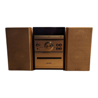
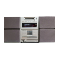
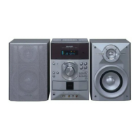
XL-MP333H/XL-MP444H
8 – 4
IC601 VHiLC75341M-1: Signal Control (LC75341M)
IC603 VHiLC75341M-1: Signal Control (LC75341M) [XL-MP444H Only]
In this unit, the terminal with asterisk mark (*) is (open) terminal which is not connected to the outside.
IC601 VHiLC75341M-1: Signal Control (LC75341M)
IC603 VHiLC75341M-1: Signal Control (LC75341M) [XL-MP444H Only]
Pin No. Terminal Name Function
1 DI Serial data and clock input pin for con-
trol.
2 CE Chip enable pin.
Data written into an internal latch in a
timing of "H" to "L".
Each analog switch is activated.
Data transfer enabled at "H" level.
3 VSS Ground pin.
4 LOUT Bass band filter comprising
capacitor and resistor connection pin
and bass/treble output pin.
5 LBASS Bass band filter comprising capacitor
and resistor connection pin.
6 LTRE Treble band filter comprising capacitor
and resistor connection pin.
7 LIN Volume + equaliser output pin.
8 LSEL0 Input selector output pin.
9 L4 Input signal pin.
10* L3 Input signal pin.
11 L2 Input signal pin.
12 L1 Input signal pin.
Pin No. Terminal Name Function
13 R1 Input signal pin.
14 R2 Input signal pin.
15* R3 Input signal pin.
16 R4 Input signal pin.
17 RSEL0 Input selector output pin.
18 RIN Volume + equaliser output pin
19 RTRE Treble band filter comprising capacitor
and resistor connection pin.
20 RBASS Bass band filter comprising capacitor
and resistor connection pin.
21 ROUT Bass band filter comprising capacitor
and resistor connection pin and bass/
treble output pin.
22 VREF 0.5x VDD voltage generation block
for analog ground. Capacitor of sev-
eral 10µF to be connected between
VREF and AWSS (VSS) as a counter-
measure against power ripple.
23 VDD Supply pin
24 CL Serial data and clock input pin for con-
trol.
19
20 21
22
23
24
1
2
3
45678
9
10
11
12
13
14
15
16
1817
LVref
RVref
CONTROL
CIRCUIT
LOGIC
CIRCUIT
CONTROL
CIRCUIT
LOUT
LBASS
LIN
LSEL0
L4
L3
L2
L1
R1
R2
R3
R4
RSEL0
RIN
RTRE
LTRE
RBASS
ROUT
VREF
VDD
CL
DI
CE
VSS
CCB
INTERFACE
Figure 2 BLOCK DIAGRAM OF IC
 Loading...