XV-Cl
E
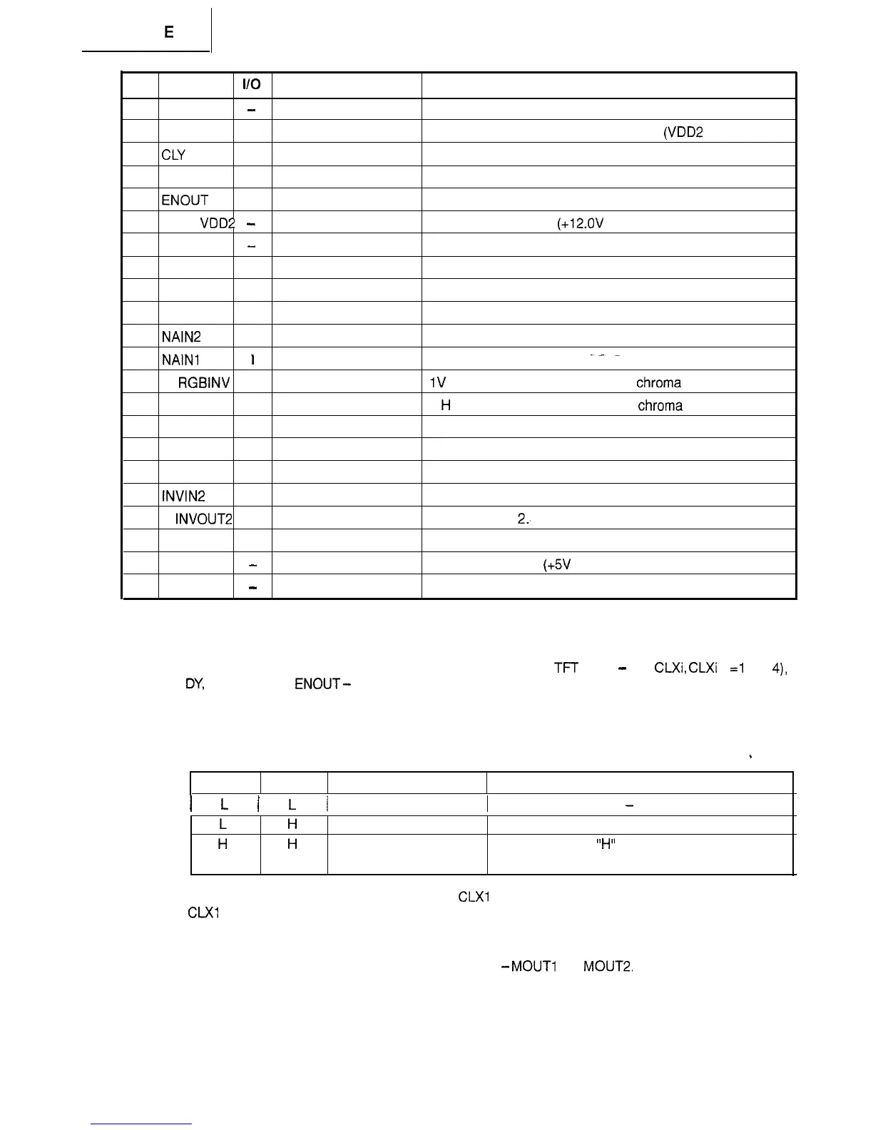
No.
Pin name
I/O Connection
Function
43 DGND
-
Power.
High-voltage power ground (OV).
44 DY 0
Output to TFT panel.
TFT panel’s Y-direction shift data output
(VDD2
line).
45
CLY
0
Output to TFT panel. TFT panel’s Y-direction transfer clock output (VDD2 line).
46 CLY
0
Output to TFT panel. TFT panel’s Y-direction transfer clock output (VDD2 line).
47
ENOUT
0
Output to TFT panel.
TFT panel’s enable signal output (VDD2 line).
48
VDD2
-
Power.
High-voltage power 2
(+12.OV
typical).
49 DGND
-
Power.
High-voltage ground (OV).
50 TEST6
I
Test terminal input.
51 OE
I
Output enable control input.
52 NAOUT 0
NAND output.
53
NAIN2
I
NAND input 2.
54 NAlNl
I
NAND input 1.
.--
55
RGBINV
0
1
V
inverted signal output (output to
chroma
IC).
56 FRP 0
1
H
inverted signal output (output to
chroma
IC).
57 CSYNC
I
Composite sync signal input.
58 MVSYNC 0
Vertical sync signal monitor output.
59 VLS 0 Output to video circuit.
Video level setting signal output for WIDE mode.
60
lNVlN2
I
lnverter input 2.
61
INVOUT2
0
lnverter output
2..
62 MFS 0 Field ID signal monitor output.
63 VCC
-
Power. Logic circuit power
(+5V
typical).
64 GND
-
Power.
Logic circuit power ground (OV).
l
The GND and DGND pins are interconnected inside the chip with a resistor in between. Be sure to keep
both pins at the same potential.
l
When the OE input level gets low, all the output signals to the
TFT
panel
-
DX,
CLXi,
CLXi
(i
=l
thru
4),
DY,
CLY, CLY, and ENOUT
-
come to low level too.
l
Be sure to fix the non-used inverter input and NAND input at the high or low level.
l
Switching between the VIDEO and WIDE modes goes as follows depending on the WMODE and
VMODE input levels. L: Low level, H: High level.
5
WMODE VMODE
Display mode
Remarks
I
L
I
L
/
NTSC
L
H
H
Intermittent PAL
H
Letter box (NTSC)
VLS: During the
“H”
period, the black-level video
signal is put into the TFT panel.
l
In the power-saving mode with no display, the CLXl thru CLX4 signals are all at low level, whereas the
CLXl thru CLX4 signals all at high level.
l
Keep all the test terminal inputs at low level.
l
Keep open the test terminal reference signal outputs
-
MOUTl and
MOUT2.
30
 Loading...